Table 37 – Xilinx DS610 User Manual
Page 45
Spartan-3A DSP FPGA Family: DC and Switching Characteristics
DS610 (v3.0) October 4, 2010
Product Specification
45
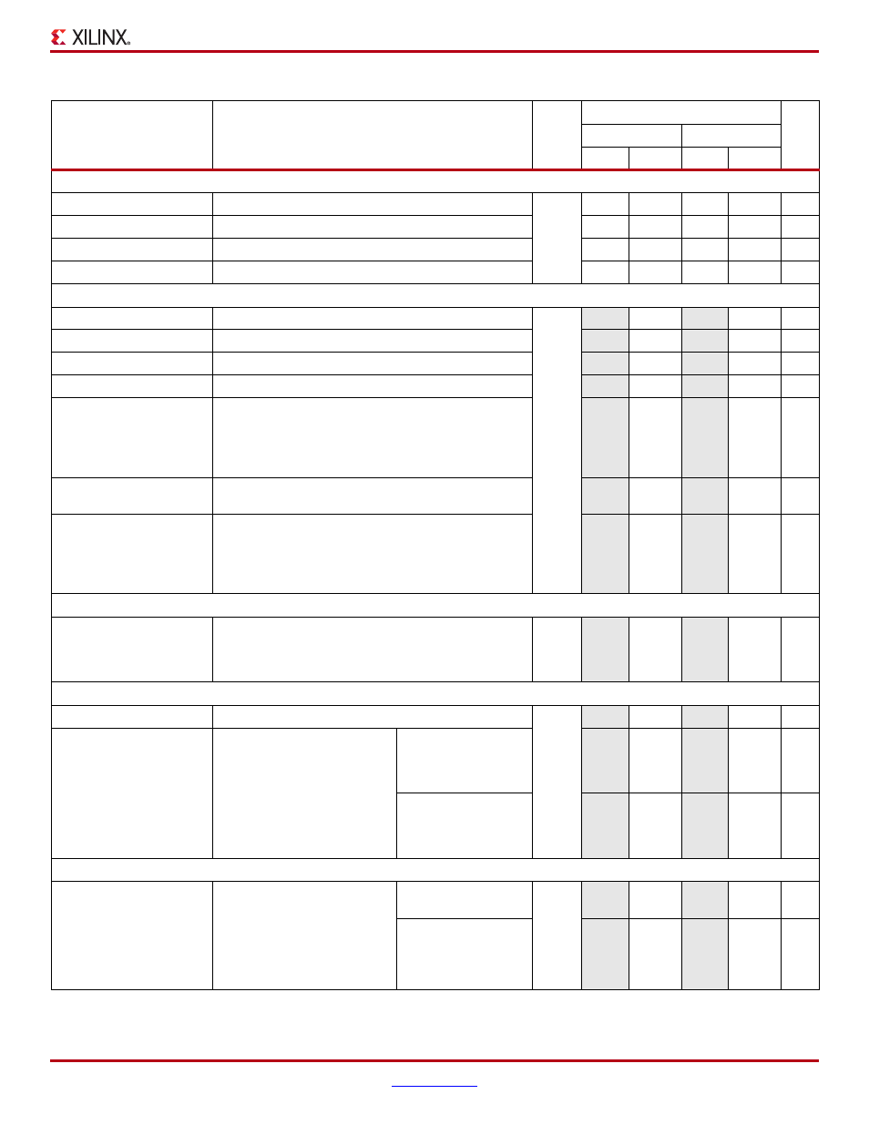
Table 37: Switching Characteristics for the DLL
Symbol
Description
Device
Speed Grade
Units
-5
-4
Min
Max
Min
Max
Output Frequency Ranges
CLKOUT_FREQ_CLK0
Frequency for the CLK0 and CLK180 outputs
All
5
280
5
250
MHz
CLKOUT_FREQ_CLK90
Frequency for the CLK90 and CLK270 outputs
5
200
5
200
MHz
CLKOUT_FREQ_2X
Frequency for the CLK2X and CLK2X180 outputs
10
334
10
334
MHz
CLKOUT_FREQ_DV
Frequency for the CLKDV output
0.3125
186
0.3125
166
MHz
Output Clock Jitter
CLKOUT_PER_JITT_0
Period jitter at the CLK0 output
All
–
±100
–
±100
ps
CLKOUT_PER_JITT_90
Period jitter at the CLK90 output
–
±150
–
±150
ps
CLKOUT_PER_JITT_180
Period jitter at the CLK180 output
–
±150
–
±150
ps
CLKOUT_PER_JITT_270
Period jitter at the CLK270 output
–
±150
–
±150
ps
CLKOUT_PER_JITT_2X
Period jitter at the CLK2X and CLK2X180 outputs
–
±[0.5%
of
CLKIN
period
+ 100]
–
±[0.5%
of
CLKIN
period
+ 100]
ps
CLKOUT_PER_JITT_DV1
Period jitter at the CLKDV output when performing
integer division
–
±150
–
±150
ps
CLKOUT_PER_JITT_DV2
Period jitter at the CLKDV output when performing
non-integer division
–
±[0.5%
of
CLKIN
period
+ 100]
–
±[0.5%
of
CLKIN
period
+ 100]
ps
Duty Cycle
CLKOUT_DUTY_CYCLE_
DLL
Duty cycle variation for the CLK0, CLK90, CLK180,
CLK270, CLK2X, CLK2X180, and CLKDV outputs,
including the BUFGMUX and clock tree duty-cycle
distortion
All
–
±[1% of
CLKIN
period
+ 350]
–
±[1% of
CLKIN
period
+ 350]
ps
Phase Alignment
CLKIN_CLKFB_PHASE
Phase offset between the CLKIN and CLKFB inputs
All
–
±150
–
±150
ps
CLKOUT_PHASE_DLL
Phase offset between DLL
outputs
CLK0 to CLK2X
(not CLK2X180)
–
±[1% of
CLKIN
period
+ 100]
–
±[1% of
CLKIN
period
+ 100]
ps
All others
–
±[1% of
CLKIN
period
+ 150]
–
±[1% of
CLKIN
period
+ 150]
ps
Lock Time
LOCK_DLL
When using the DLL alone:
The time from deassertion at
the DCM’s Reset input to the
rising transition at its LOCKED
output. When the DCM is
locked, the CLKIN and CLKFB
signals are in phase
5 MHz < FCLKIN <
15 MHz
All
–
5
–
5
ms
FCLKIN > 15 MHz
–
600
–
600
µs