Dna port timing – Xilinx DS610 User Manual
Page 49
Spartan-3A DSP FPGA Family: DC and Switching Characteristics
DS610 (v3.0) October 4, 2010
Product Specification
49
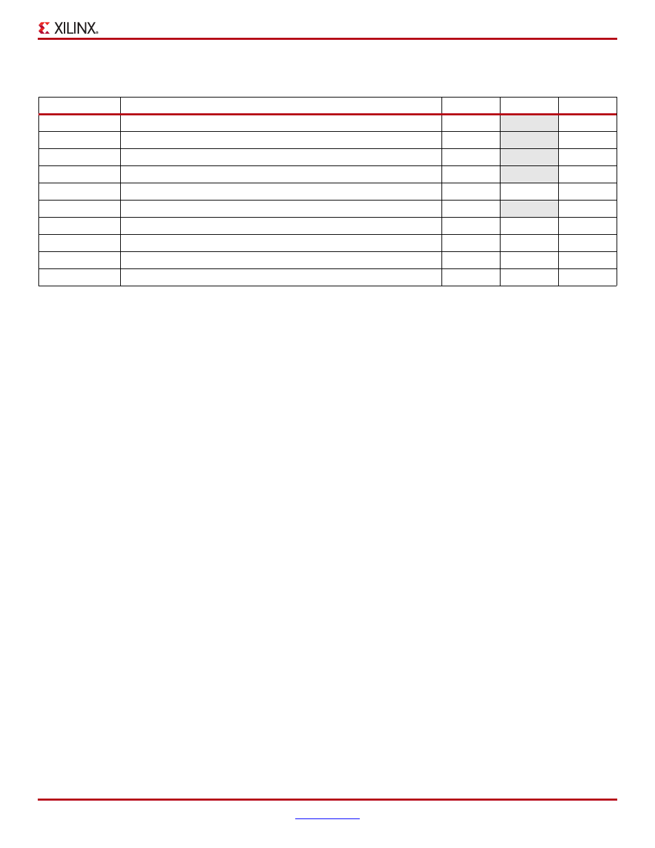
DNA Port Timing
Table 43: DNA_PORT Interface Timing
Symbol
Description
Min
Max
Units
T
DNASSU
Setup time on SHIFT before the rising edge of CLK
1.0
–
ns
T
DNASH
Hold time on SHIFT after the rising edge of CLK
0.5
–
ns
T
DNADSU
Setup time on DIN before the rising edge of CLK
1.0
–
ns
T
DNADH
Hold time on DIN after the rising edge of CLK
0.5
–
ns
T
DNARSU
Setup time on READ before the rising edge of CLK
5.0
10,000
ns
T
DNARH
Hold time on READ after the rising edge of CLK
0.0
–
ns
T
DNADCKO
Clock-to-output delay on DOUT after rising edge of CLK
0.5
1.5
ns
T
DNACLKF
CLK frequency
0.0
100
MHz
T
DNACLKH
CLK High time
1.0
∞
ns
T
DNACLKL
CLK Low time
1.0
∞
ns
Notes:
1.
The minimum READ pulse width is 5 ns, and the maximum READ pulse width is 10
μs.