Digital frequency synthesizer (dfs), Table 38 – Xilinx DS610 User Manual
Page 46
Spartan-3A DSP FPGA Family: DC and Switching Characteristics
DS610 (v3.0) October 4, 2010
Product Specification
46
Digital Frequency Synthesizer (DFS)
Delay Lines
DCM_DELAY_STEP
Finest delay resolution, averaged over all steps
All
15
35
15
35
ps
Notes:
1.
The numbers in this table are based on the operating conditions set forth in
2.
Indicates the maximum amount of output jitter that the DCM adds to the jitter on the CLKIN input.
3.
For optimal jitter tolerance and faster lock time, use the CLKIN_PERIOD attribute.
4.
Some jitter and duty-cycle specifications include 1% of input clock period or 0.01 UI. For example, the data sheet specifies a maximum jitter
of ±[1% of CLKIN period + 150]. Assume the CLKIN frequency is 100 MHz. The equivalent CLKIN period is 10 ns and 1% of 10 ns is 0.1 ns
or 100 ps. According to the data sheet, the maximum jitter is ±[100 ps + 150 ps] = ±250 ps, averaged over all steps.
5.
The typical delay step size is 23 ps.
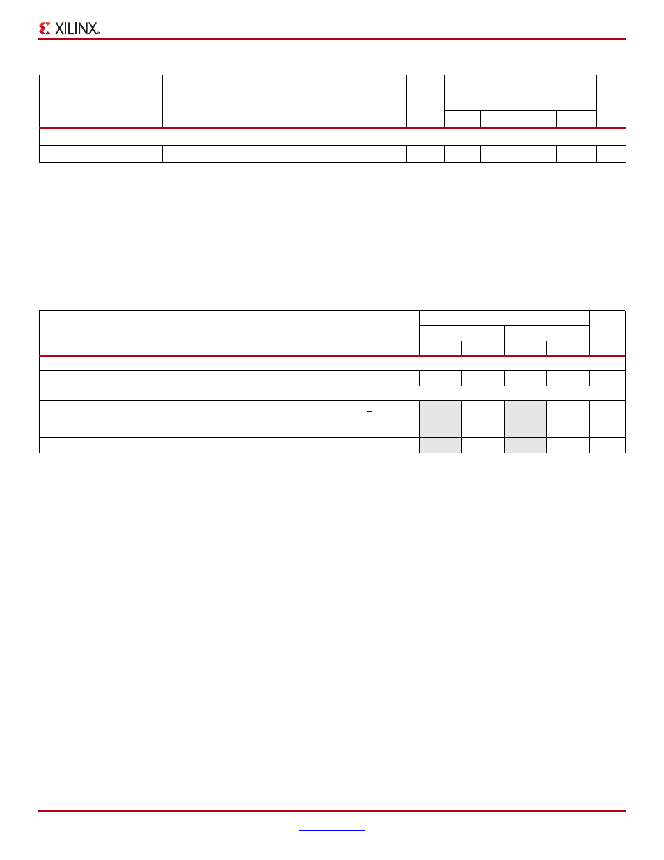
Table 38: Recommended Operating Conditions for the DFS
Symbol
Description
Speed Grade
Units
-5
-4
Min
Max
Min
Max
Input Frequency Ranges
F
CLKIN
CLKIN_FREQ_FX
Frequency for the CLKIN input
0.2
333
0.2
333
MHz
Input Clock Jitter Tolerance
CLKIN_CYC_JITT_FX_LF
Cycle-to-cycle jitter at the
CLKIN input, based on CLKFX
output frequency
F
CLKFX
< 150 MHz
–
±300
–
±300
ps
CLKIN_CYC_JITT_FX_HF
F
CLKFX
> 150 MHz
–
±150
–
±150
ps
CLKIN_PER_JITT_FX
Period jitter at the CLKIN input
–
±1
–
±1
ns
Notes:
1.
DFS specifications apply when either of the DFS outputs (CLKFX or CLKFX180) are used.
2.
If both DFS and DLL outputs are used on the same DCM, follow the more restrictive CLKIN_FREQ_DLL specifications in
.
3.
CLKIN input jitter beyond these limits may cause the DCM to lose lock.
4.
The DCM specifications are guaranteed when both adjacent DCMs are locked.
5.
To support double the maximum effective F
CLKIN
limit, set the CLKIN_DIVIDE_BY_2 attribute to TRUE. This attribute divides the incoming
clock frequency by two as it enters the DCM.
Table 37: Switching Characteristics for the DLL (Cont’d)
Symbol
Description
Device
Speed Grade
Units
-5
-4
Min
Max
Min
Max