Xilinx DS610 User Manual
Page 25
Spartan-3A DSP FPGA Family: DC and Switching Characteristics
DS610 (v3.0) October 4, 2010
Product Specification
25
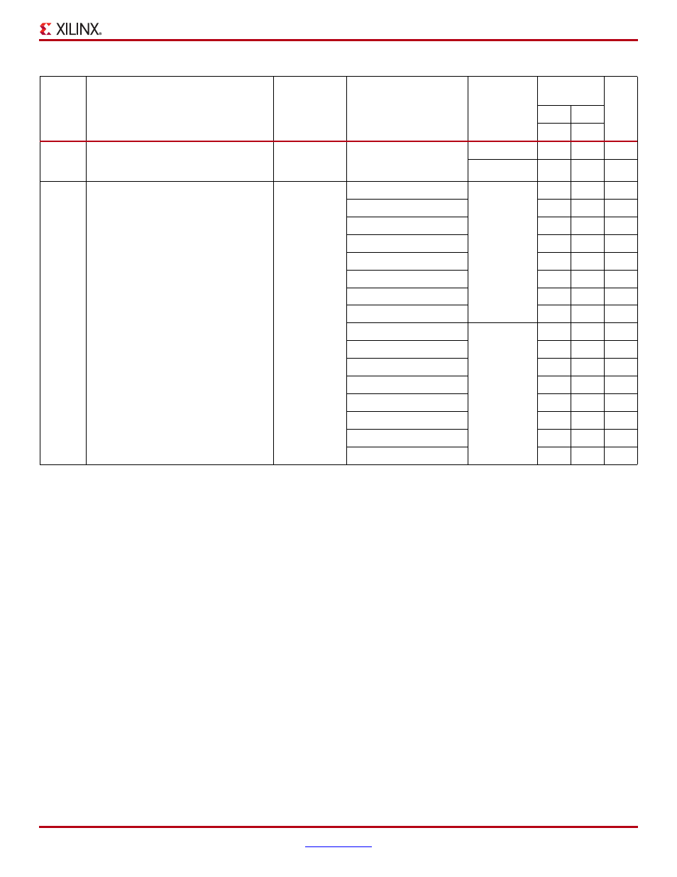
T
IOPLI
The time it takes for data to travel from
the Input pin through the IFF latch to the
I output with no input delay programmed
LVCMOS25
0
XC3SD1800A
1.79
2.04
ns
XC3SD3400A
1.65
2.11
ns
T
IOPLID
The time it takes for data to travel from
the Input pin through the IFF latch to the
I output with the input delay programmed
LVCMOS25
1
XC3SD1800A
2.23
2.47
ns
2
2.81
3.06
ns
3
3.39
3.86
ns
4
3.89
4.43
ns
5
3.83
4.39
ns
6
4.61
5.32
ns
7
5.40
6.24
ns
8
5.93
6.86
ns
1
XC3SD3400A
2.21
2.67
ns
2
2.71
3.25
ns
3
3.58
4.04
ns
4
4.15
4.62
ns
5
4.03
4.49
ns
6
4.57
5.31
ns
7
5.34
6.18
ns
8
5.84
6.78
ns
Notes:
1.
The numbers in this table are tested using the methodology presented in
and are based on the operating conditions set forth in
.
2.
This propagation time requires adjustment whenever a signal standard other than LVCMOS25 is assigned to the data Input. When this is
true, add the appropriate Input adjustment from
Table 21: Propagation Times for the IOB Input Path (Cont’d)
Symbol
Description
Conditions
DELAY_VALUE
Device
Speed
Grade
Units
-5
-4
Max
Max