Xilinx DS610 User Manual
Page 23
Spartan-3A DSP FPGA Family: DC and Switching Characteristics
DS610 (v3.0) October 4, 2010
Product Specification
23
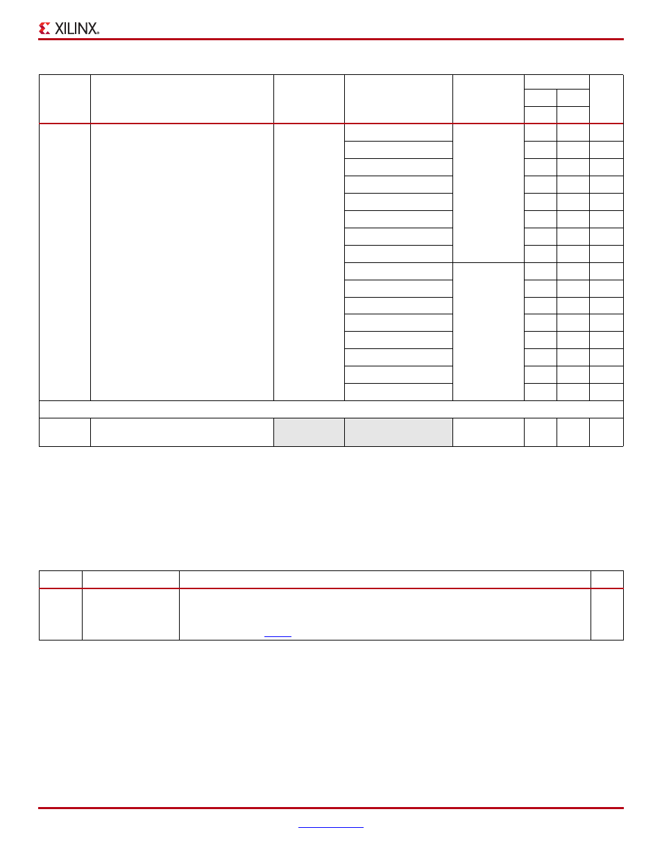
T
IOICKPD
Time from the active transition at the
ICLK input of the Input Flip-Flop (IFF) to
the point where data must be held at the
Input pin. The Input Delay is
programmed.
LVCMOS25
1
XC3SD1800A
–1.40 –1.40
ns
2
–2.11 –2.11
ns
3
–2.48 –2.48
ns
4
–2.77 –2.77
ns
5
–2.62 –2.62
ns
6
–3.06 –3.06
ns
7
–3.42 –3.42
ns
8
–3.65 –3.65
ns
1
XC3SD3400A
–1.31 –1.31
ns
2
–1.88 –1.88
ns
3
–2.44 –2.44
ns
4
–2.89 –2.89
ns
5
–2.83 –2.83
ns
6
–3.33 –3.33
ns
7
–3.63 –3.63
ns
8
–3.96 –3.96
ns
Set/Reset Pulse Width
T
RPW_IOB
Minimum pulse width to SR control input
on IOB
–
–
All
1.33
1.61
ns
Notes:
1.
The numbers in this table are tested using the methodology presented in
and are based on the operating conditions set forth in
.
2.
This setup time requires adjustment whenever a signal standard other than LVCMOS25 is assigned to the data Input. If this is true, add the
appropriate Input adjustment from
3.
These hold times require adjustment whenever a signal standard other than LVCMOS25 is assigned to the data Input. If this is true, subtract
the appropriate Input adjustment from
. When the hold time is negative, it is possible to change the data before the clock’s active
edge.
Table 20: Sample Window (Source Synchronous)
Symbol
Description
Max
Units
T
SAMP
Setup and hold
capture window of
an IOB flip-flop.
The input capture sample window value is highly specific to a particular application, device,
package, I/O standard, I/O placement, DCM usage, and clock buffer. Please consult the
appropriate Xilinx Answer Record for application-specific values.
•
Answe
ps
Table 19: Setup and Hold Times for the IOB Input Path (Cont’d)
Symbol
Description
Conditions
DELAY_
VALUE
Device
Speed
Units
-5
-4
Min
Min