I/o timing, Pin-to-pin clock-to-output times – Xilinx DS610 User Manual
Page 20
Spartan-3A DSP FPGA Family: DC and Switching Characteristics
DS610 (v3.0) October 4, 2010
Product Specification
20
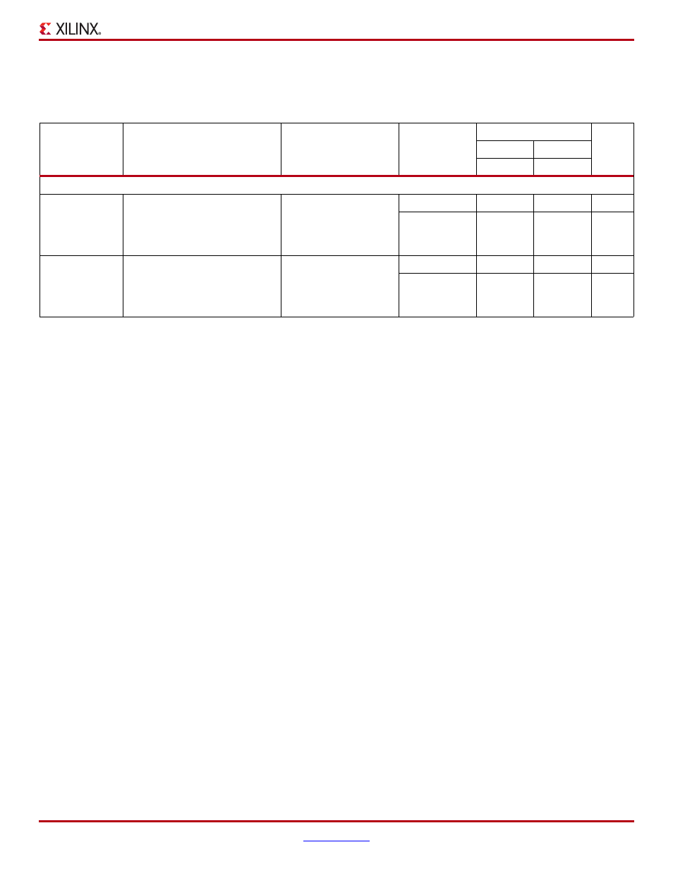
I/O Timing
Pin-to-Pin Clock-to-Output Times
Table 17: Pin-to-Pin Clock-to-Output Times for the IOB Output Path
Symbol
Description
Conditions
Device
Speed Grade
Units
-5
-4
Max
Max
Clock-to-Output Times
T
ICKOFDCM
When reading from the Output
Flip-Flop (OFF), the time from the
active transition on the Global
Clock pin to data appearing at the
Output pin. The DCM is in use.
LVCMOS25
, 12 mA
output drive, Fast slew
rate, with DCM
XC3SD1800A
3.28
3.51
ns
XC3SD3400A
3.36
3.82
ns
T
ICKOF
When reading from OFF, the time
from the active transition on the
Global Clock pin to data appearing
at the Output pin. The DCM is not
in use.
LVCMOS25
, 12 mA
output drive, Fast slew
rate, without DCM
XC3SD1800A
5.23
5.58
ns
XC3SD3400A
5.51
6.13 ns
Notes:
1.
The numbers in this table are tested using the methodology presented in
and are based on the operating conditions set forth in
.
2.
This clock-to-output time requires adjustment whenever a signal standard other than LVCMOS25 is assigned to the Global Clock Input or a
standard other than LVCMOS25 with 12 mA drive and Fast slew rate is assigned to the data Output. If the former is true, add the appropriate
Input adjustment from
. If the latter is true, add the appropriate Output adjustment from
3.
DCM output jitter is included in all measurements.