Differential output pairs – Xilinx DS610 User Manual
Page 17
Spartan-3A DSP FPGA Family: DC and Switching Characteristics
DS610 (v3.0) October 4, 2010
Product Specification
17
Differential Output Pairs
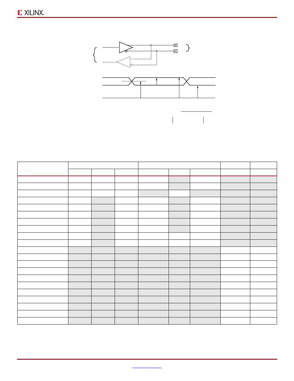
X-Ref Target - Figure 4
Figure 4: Differential Output Voltages
Table 13: DC Characteristics of User I/Os Using Differential Signal Standards
IOSTANDARD Attribute
V
OD
V
OCM
V
OH
V
OL
Min (mV)
Typ (mV)
Max (mV)
Min (V)
Typ (V)
Max (V)
Min (V)
Max (V)
LVDS_25
247
350
454
1.125
–
1.375
–
–
LVDS_33
247
350
454
1.125
–
1.375
–
–
BLVDS_25
240
350
460
–
1.30
–
–
–
MINI_LVDS_25
300
–
600
1.0
–
1.4
–
–
MINI_LVDS_33
300
–
600
1.0
–
1.4
–
–
RSDS_25
100
–
400
1.0
–
1.4
–
–
RSDS_33
100
–
400
1.0
–
1.4
–
–
TMDS_33
400
–
800
V
CCO
– 0.405
–
V
CCO
– 0.190
–
–
PPDS_25
100
–
400
0.5
0.8
1.4
–
–
PPDS_33
100
–
400
0.5
0.8
1.4
–
–
DIFF_HSTL_I_18
–
–
–
–
–
–
V
CCO
– 0.4
0.4
DIFF_HSTL_II_18
–
–
–
–
–
–
V
CCO
– 0.4
0.4
DIFF_HSTL_III_18
–
–
–
–
–
–
V
CCO
– 0.4
0.4
DIFF_HSTL_I
–
–
–
–
–
–
V
CCO
– 0.4
0.4
DIFF_HSTL_III
–
–
–
–
–
–
V
CCO
– 0.4
0.4
DIFF_SSTL18_I
–
–
–
–
–
–
V
TT
+ 0.475
V
TT
– 0.475
DIFF_SSTL18_II
–
–
–
–
–
–
V
TT
+ 0.603
V
TT
– 0.603
DIFF_SSTL2_I
–
–
–
–
–
–
V
TT
+ 0.61
V
TT
– 0.61
DIFF_SSTL2_II
–
–
–
–
–
–
V
TT
+ 0.81
V
TT
– 0.81
DIFF_SSTL3_I
–
–
–
–
–
–
V
TT
+ 0.6
V
TT
- 0.6
DIFF_SSTL3_II
–
–
–
–
–
–
V
TT
+ 0.8
V
TT
- 0.8
Notes:
1.
The numbers in this table are based on the conditions set forth in
and
.
2.
"External Termination Requirements for Differential I/O."
3.
Output voltage measurements for all differential standards are made with a termination resistor (R
T
) of 100
Ω across the N and P pins of the differential signal pair.
4.
At any given time, no more than two of the following differential output standards can be assigned to an I/O bank: LVDS_25, RSDS_25, MINI_LVDS_25, PPDS_25 when
V
CCO
=2.5V, or LVDS_33, RSDS_33, MINI_LVDS_33, TMDS_33, PPDS_33 when V
CCO
= 3.3V
V
OUTN
V
OUTP
GND level
50%
V
OCM
V
OCM
V
OD
V
OL
V
OH
V
OUTP
Internal
Logic
V
OUTN
N
P
= Output common mode voltage =
2
V
OUTP
+ V
OUTN
V
OD
= Output differential voltage =
V
OH
= Output voltage indicating a High logic level
V
OL
= Output voltage indicating a Low logic level
V
OUTP
- V
OUTN
Differential
I/O Pair Pins
DS312-3_03_090510