Ieee 1149.1/1532 jtag test access port timing – Xilinx DS610 User Manual
Page 60
Spartan-3A DSP FPGA Family: DC and Switching Characteristics
DS610 (v3.0) October 4, 2010
Product Specification
60
IEEE 1149.1/1532 JTAG Test Access Port Timing
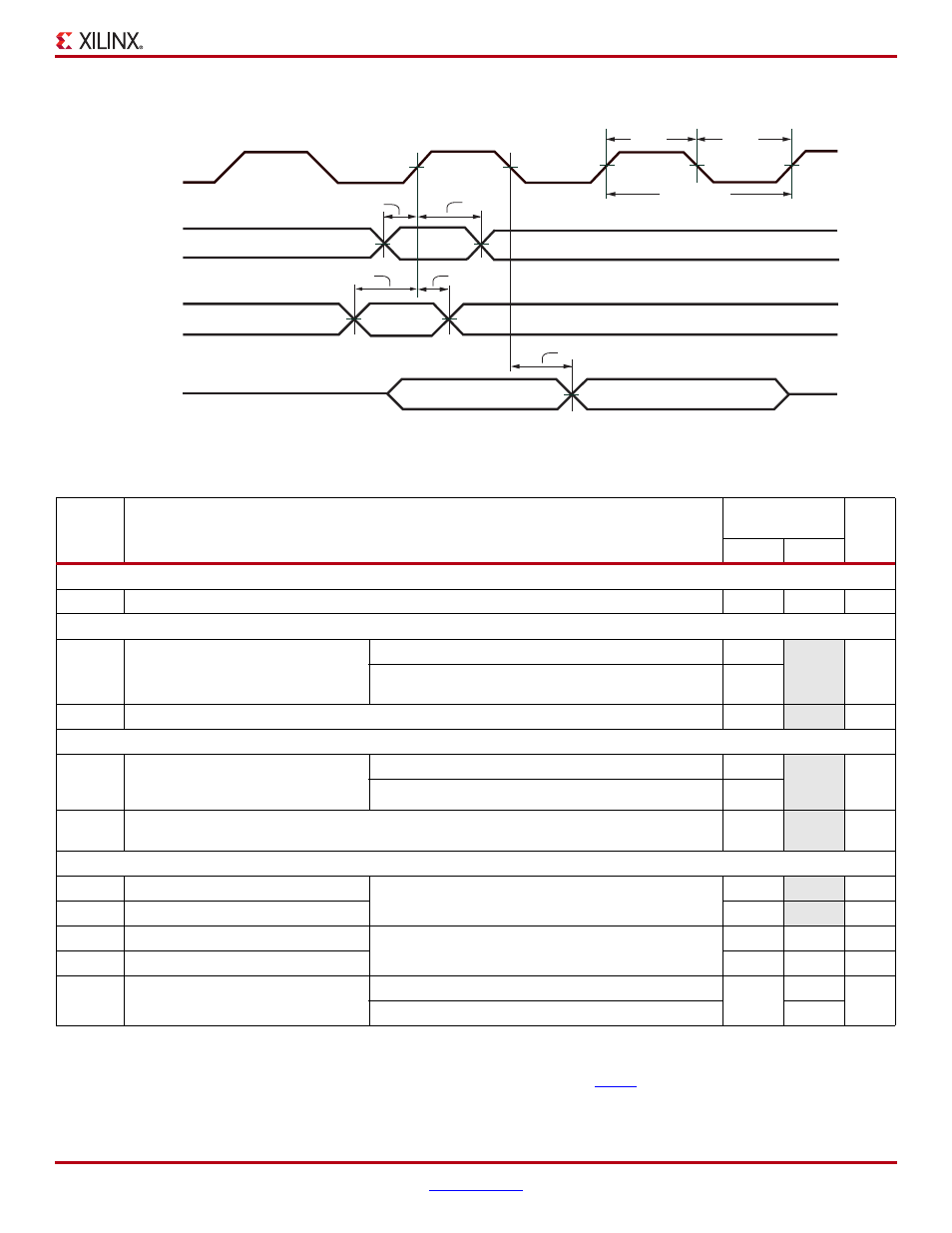
X-Ref Target - Figure 15
Figure 15: JTAG Waveforms
Table 56: Timing for the JTAG
Test Access Port
Symbol
Description
All Speed
Grades
Units
Min
Max
Clock-to-Output Times
T
TCKTDO
The time from the falling transition on the TCK pin to data appearing at the TDO pin
1.0
11.0
ns
Setup Times
T
TDITCK
The time from the setup of data at the
TDI pin to the rising transition at the
TCK pin
All functions except those shown below
7.0
–
ns
Boundary scan commands
(INTEST, EXTEST, SAMPLE)
13.0
T
TMSTCK
The time from the setup of a logic level at the TMS pin to the rising transition at the TCK pin
7.0
–
ns
Hold Times
T
TCKTDI
The time from the rising transition at
the TCK pin to the point when data is
last held at the TDI pin
All functions except those shown below
0
–
ns
Configuration commands (CFG_IN, ISC_PROGRAM)
3.5
T
TCKTMS
The time from the rising transition at the TCK pin to the point when a logic level is last held at the
TMS pin
0
–
ns
Clock Timing
T
CCH
The High pulse width at the TCK pin
All functions except ISC_DNA command
5
–
ns
T
CCL
The Low pulse width at the TCK pin
5
–
ns
T
CCHDNA
The High pulse width at the TCK pin
During ISC_DNA command
10
10,000
ns
T
CCLDNA
The Low pulse width at the TCK pin
10
10,000
ns
F
TCK
Frequency of the TCK signal
BYPASS or HIGHZ instructions
0
33
MHz
All operations except for BYPASS or HIGHZ instructions
20
Notes:
1.
The numbers in this table are based on the operating conditions set forth in
2.
For details on JTAG, see Chapter 9, “JTAG Configuraton Mode and Boundary-Scan” in
Spartan-3 Generation Configuration User
Guide.
TCK
T
TMSTCK
TMS
TDI
TDO
(Input)
(Input)
(Input)
(Output)
T
TCKTMS
T
TCKTDI
T
TCKTDO
T
TDITCK
DS099_06_090610
T
CCH
T
CCL
1/F
TCK