NEC PD750008 User Manual
Page 89
69
CHAPTER 5 PERIPHERAL HARDWARE FUNCTIONS
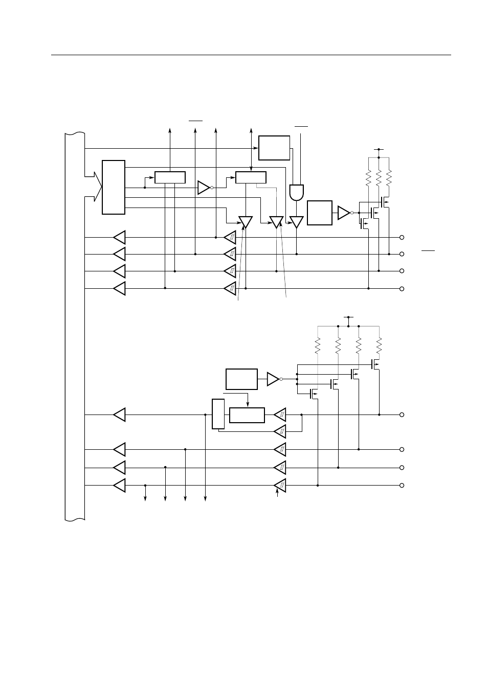
Figure 5-2. Configurations of Ports 0 and 1
Internal bus
8
CSIM
Selector
Selector
P01
output
latch
Internal
SCK
SI
SCK
SO
INT4
V
DD
Pull-up
resistor
P-ch
P00/INT4
P01/SCK
P02/SO/SB0
P03/SI/SB1
Bit 0 of
POGA
Input buffer
Output buffer which can
be switched to either
push-pull output or N-ch
open-drain output
Pull-up
resistor
V
DD
P-ch
P10/INT0
P11/INT1
P12/INT2
P13/ TI0
Bit 1 of
POGA
Input buffer
Φ
or f
X
/64
Input buffer with hysteresis
TI0
INT2 INT1 INT0
Noise
eliminator
Selector
N-ch
open drain