NEC PD750008 User Manual
Page 60
4 0
µPD750008 USER'S MANUAL
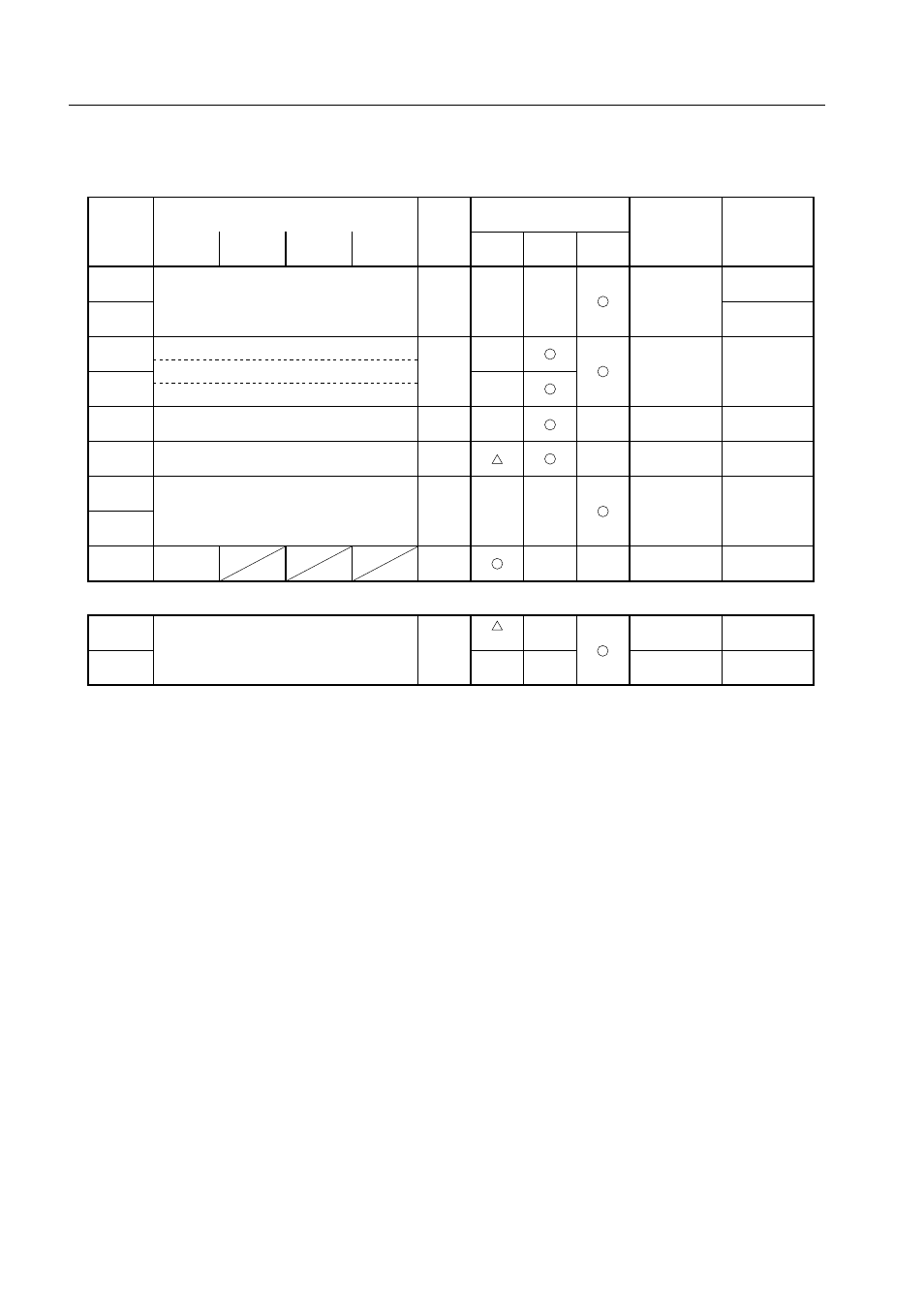
Figure 3-7. µPD750008 I/O Map (1/5)
Notes 1. Can be manipulated separately as the RBS and MBS in 4-bit units.
Can also be manipulated as the BS in 8-bit units.
Use SEL MBn and SEL RBn instructions to write data to MBS and RBS respectively.
2. WDTM: Watchdog timer enable flag (W); cannot be cleared by an instruction.
F80H
F82H
F83H
F85H
F86H
F8BH
F98H
Address
b3
b2
b1
b0
Hardware name (symbol)
R/ W
1 bit
4 bits
8 bits
Remarks
Number of bits that can be
manipulated
R/ W
R
–
–
–
–
–
–
Note 1
Bit
manipulation
addressing
Stack pointer (SP)
Register bank selection register (RBS)
Bank selection register (BS)
Memory bank selection register (MBS)
Basic interval timer mode register (BTM)
Basic interval timer (BT)
WDTM
Bit 0 is fixed
to 0.
Only bit 3 can
be manipulated.
W
W
R
–
–
–
–
–
mem.bit
mem.bit
–
Clock mode register (WM)
R/ W
–
–
–
(R)
–
mem.bit
Only bit 3 can
be tested.
F84H
Stack bank selection register (SBS)
R/W
–
mem.bit
–
Note 2