Pca9665, Nxp semiconductors – NXP Semiconductors PCA9665 User Manual
Page 76

PCA9665_2
© NXP B.V. 2006. All rights reserved.
Product data sheet
Rev. 02 — 7 December 2006
76 of 91
NXP Semiconductors
PCA9665
Fm+ parallel bus to I
2
C-bus controller
[1]
Minimum SCL clock frequency is limited by the bus time-out feature, which resets the serial bus interface if either SDA or SCL is held
LOW for a minimum of 25 ms. Disable bus time-out feature for DC operation.
[2]
t
VD;ACK
= time for Acknowledgement signal from SCL LOW to SDA (out) LOW.
[3]
t
VD;DAT
= minimum time for SDA data out to be valid following SCL LOW.
[4]
C
b
= total capacitance of one bus line in pF.
[5]
A master device must internally provide a hold time of at least 300 ns for the SDA signal (refer to the V
IL
of the SCL signal) in order to
bridge the undefined region SCL’s falling edge.
[6]
The maximum t
f
for the SDA and SCL bus lines is specified at 300 ns. The maximum fall time for the SDA output stage t
f
is specified at
250 ns. This allows series protection resistors to be connected between the SDA and the SCL pins and the SDA/SCL bus lines without
exceeding the maximum specified t
f
.
[7]
Input filters on the SDA and SCL inputs suppress noise spikes less than 50 ns.
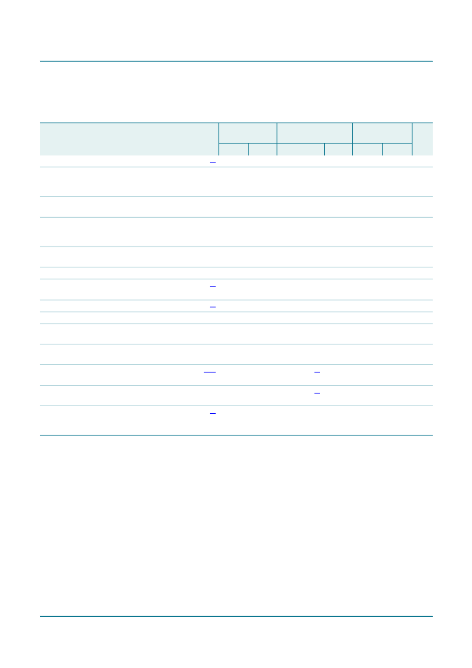
Table 51.
I
2
C-bus frequency and timing specifications
All the timing limits are valid within the operating supply voltage and ambient temperature range; V
DD
= 2.5 V
±
0.2 V and
3.3 V
±
0.3 V; T
amb
=
−
40
°
C to +85
°
C; and refer to V
IL
and V
IH
with an input voltage of V
SS
to V
DD
.
Symbol
Parameter
Conditions
Standard-mode
I
2
C-bus
Fast-mode I
2
C-bus
Fast-mode Plus
I
2
C-bus
Unit
Min
Max
Min
Max
Min
Max
f
SCL
SCL clock frequency
0
100
0
400
0
1000
kHz
t
BUF
bus free time between a
STOP and START
condition
4.7
-
1.3
-
0.5
-
µ
s
t
HD;STA
hold time (repeated)
START condition
4.0
-
0.6
-
0.26
-
µ
s
t
SU;STA
set-up time for a
repeated START
condition
4.7
-
0.6
-
0.26
-
µ
s
t
SU;STO
set-up time for STOP
condition
4.0
-
0.6
-
0.26
-
µ
s
t
HD;DAT
data hold time
0
-
0
-
0
-
ns
t
VD;ACK
data valid acknowledge
time
0.05
3.45
0.05
0.9
0.05
0.45
µ
s
t
VD;DAT
data valid time
50
-
50
-
50
-
ns
t
SU;DAT
data set-up time
250
-
100
-
50
-
ns
t
LOW
LOW period of the SCL
clock
4.7
-
1.3
-
0.5
-
µ
s
t
HIGH
HIGH period of the SCL
clock
4.0
-
0.6
-
0.26
-
µ
s
t
f
fall time of both SDA and
SCL signals
-
300
20 + 0.1C
b
300
-
120
ns
t
r
rise time of both SDA and
SCL signals
-
1000
20 + 0.1C
b
300
-
120
ns
t
SP
pulse width of spikes that
must be suppressed by
the input filter
-
50
-
50
-
50
ns
