Figure 7, Pca9665, Nxp semiconductors – NXP Semiconductors PCA9665 User Manual
Page 19: Fm+ parallel bus to i, C-bus controller
PCA9665_2
© NXP B.V. 2006. All rights reserved.
Product data sheet
Rev. 02 — 7 December 2006
19 of 91
NXP Semiconductors
PCA9665
Fm+ parallel bus to I
2
C-bus controller
(1) See
(2) Defined state when a single byte is sent and an ACK is received.
(3) Defined state when a single byte is sent and a NACK is received.
(4) Master Receiver Byte mode is entered when MODE = 0. Master Receiver Buffered mode is entered when MODE = 1.
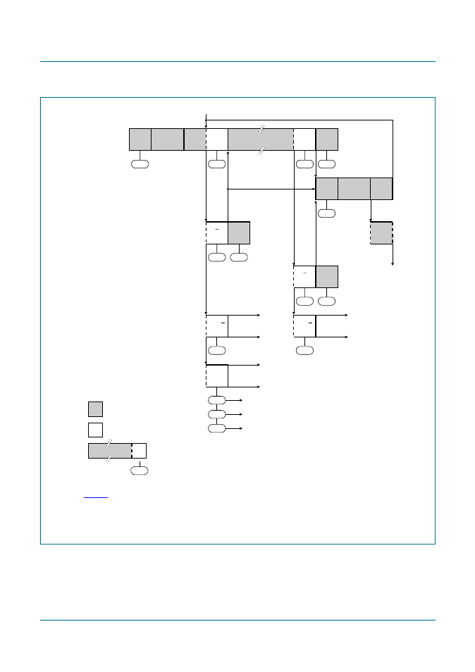
Fig 7.
Format and states in the Master Transmitter Byte mode (MODE = 0)
08h
S
SLA
W
A
DATA
A
P
18h
28h
F8h
MT
10h
S
SLA
W
R
to Master Receiver
mode entry = MR
(4)
A
P
30h
F8h
A
P
20h
F8h
002aab024
A or A
38h
other MST
continues
A or A
38h
other MST
continues
A
B0h
other MST
continues
68h
to corresponding states in Slave Transmitter mode
to corresponding states in Slave Receiver mode
successful
transmission
to a Slave Receiver
next transfer started with a
repeated START condition
Not Acknowledge received after
the slave address
Not Acknowledge received after
a data byte
arbitration lost in slave address
or data byte
arbitration lost and addressed as slave
n
This number (contained in I2CSTA) corresponds
to a defined state of the I
2
C-bus.
(1)
DATA
A
any number of data bytes and
their associated Acknowledge bits
from master to slave
from slave to master
D8h
to corresponding states in Slave Receiver mode (General Call)
(2)
(3)