3 slave receiver buffered mode, Pca9665 – NXP Semiconductors PCA9665 User Manual
Page 40

PCA9665_2
© NXP B.V. 2006. All rights reserved.
Product data sheet
Rev. 02 — 7 December 2006
40 of 91
NXP Semiconductors
PCA9665
Fm+ parallel bus to I
2
C-bus controller
8.4.3 Slave Receiver Buffered mode
In the Slave Receiver Buffered mode, a number of data bytes are received from a master
transmitter several bytes at a time (see
). To initiate the Slave Receiver Byte
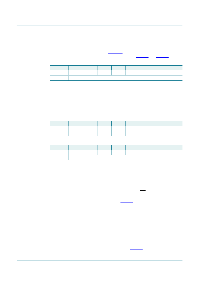
mode, I2CADR and I2CCON must be loaded as shown in
and
The upper 7 bits are the I
2
C-bus address to which PCA9665 will respond when addressed
by a master. GC is the control bit that allows the PCA9665 to respond or not to the
General Call address (00h).
When programmed to logic 1, the PCA9665 will acknowledge the General Call address.
When programmed to logic 0, the PCA9665 will not acknowledge the General Call
address.
ENSIO must be set to logic 1 to enable the I
2
C-bus interface. The AA bit must be set to
enable the PCA9665 to acknowledge its own slave address; STA, STO, and SI must be
reset.
When I2CADR and I2CCON have been initialized, the PCA9665 waits until it is addressed
by its own slave address followed by the data direction bit which must be ‘0’ (W) to operate
in the Slave Receiver mode. After its own slave address and the W bit have been
received, the Serial Interrupt flag (SI) is set, the Interrupt line (INT) goes LOW and I2CSTA
is loaded with 60h. This status code is used to vector to an interrupt service routine, and
the appropriate action to be taken is detailed in
The Slave Receiver Buffered mode may also be entered when:
•
The arbitration is lost while the PCA9665 is in the master mode. See status 68h and
D8h.
•
The General Call Address (00h) has been received (General Call address enabled
with GC = 1). See status D0h.
Appropriate actions to be taken from these status codes are also detailed in
.
The byte count register (I2CCOUNT) is programmed with the number of bytes that need
to be sent in a single sequence (BC[6:0]) as shown in
Table 37.
I2CADR initialization
Bit
7
6
5
4
3
2
1
0
Symbol
AD7
AD6
AD5
AD4
AD3
AD2
AD1
GC
Value
own slave address
X
Table 38.
I2CCON initialization
Bit
7
6
5
4
3
2
1
0
Symbol
AA
ENSIO
STA
STO
SI
-
-
MODE
Value
1
1
0
0
0
X
X
1
Table 39.
I2CCOUNT programming
Bit
7
6
5
4
3
2
1
0
Symbol
LB
BC6
BC5
BC4
BC3
BC2
BC1
BC0
Value
X
number of bytes received in a single sequence (1 byte to 68 bytes)
