Figure 12, Pca9665, Nxp semiconductors – NXP Semiconductors PCA9665 User Manual
Page 37: Fm+ parallel bus to i, C-bus controller

PCA9665_2
© NXP B.V. 2006. All rights reserved.
Product data sheet
Rev. 02 — 7 December 2006
37 of 91
NXP Semiconductors
PCA9665
Fm+ parallel bus to I
2
C-bus controller
(1) See
(2) No serial interrupt.
(3) Defined state when LB = 0 and the number of bytes received is equal to the value in I2CCOUNT register.
(4) Defined state when LB = 1 and the number of bytes received is equal to the value in I2CCOUNT register.
(5) Master Transmitter Byte mode is entered with MODE = 0. Master Transmitter Buffered mode is entered when MODE = 1.
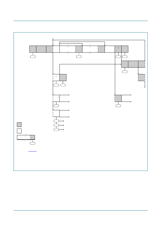
Fig 12. Format and states in the Master Receiver Buffered mode (MODE = 1)
08h
S
SLA
R
A
DATA
A
P
50h
F8h
MR
10h
S
SLA
R
W
to Master Transmitter mode
entry = MT
(5)
A
P
48h
F8h
002aab660
A
38h
other MST
continues
A or A
38h
other MST
continues
A
other MST
continues
successful
reception
from a Slave
Transmitter
next transfer
started with a
repeated START
condition
Not Acknowledge
received after
the slave address
arbitration lost in
slave address
or Acknowledge bit
arbitration lost and
addressed as slave
n
This number (contained in I2CSTA) corresponds
to a defined state of the I
2
C-bus.
(1)
DATA
A
any number of data bytes and
their associated Acknowledge bits
from master to slave
from slave to master
DATA
A
58h
(3)
(4)
B0h
68h
to corresponding states in Slave Transmitter mode
to corresponding states in Slave Receiver mode
D8h
to corresponding states in Slave Receiver mode (General Call)
(2)
DATA
A
