Maxim Integrated DS33R11 User Manual
General description, Applications, Functional diagram
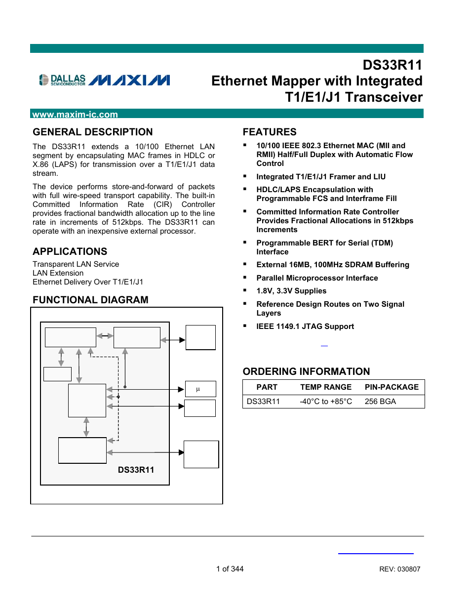
Table of contents
Document Outline
- TABLE OF CONTENTS
- 1 DESCRIPTION
- 2 FEATURE HIGHLIGHTS
- 2.1 General
- 2.2 Microprocessor Interface
- 2.3 HDLC Ethernet Mapping
- 2.4 X.86 (Link Access Protocol for SONET/SDH) Ethernet Mapping
- 2.5 Additional HDLC Controllers in the Integrated T1/E1/J1 Transceiver
- 2.6 Committed Information Rate (CIR) Controller
- 2.7 SDRAM Interface
- 2.8 MAC Interface
- 2.9 T1/E1/J1 Line Interface
- 2.10 Clock Synthesizer
- 2.11 Jitter Attenuator
- 2.12 T1/E1/J1 Framer
- 2.13 TDM Bus
- 2.14 Test and Diagnostics
- 2.15 Specifications Compliance
- 3 APPLICATIONS
- 4 ACRONYMS AND GLOSSARY
- 5 MAJOR OPERATING MODES
- 6 BLOCK DIAGRAMS
- 7 PIN DESCRIPTIONS
- 8 FUNCTIONAL DESCRIPTION
- 9 ETHERNET MAPPER
- 9.1 Ethernet Mapper Clocks
- 9.2 Resets and Low Power Modes
- 9.3 Initialization and Configuration
- 9.4 Global Resources
- 9.5 Per-Port Resources
- 9.6 Device Interrupts
- 9.7 Interrupt Information Registers
- 9.8 Status Registers
- 9.9 Information Registers
- 9.10 Serial Interface
- 9.11 Connections and Queues
- 9.12 Arbiter
- 9.13 Flow Control
- 9.14 Ethernet Interface Port
- 9.15 Ethernet MAC
- 9.16 BERT in the Ethernet Mapper
- 9.17 Transmit Packet Processor
- 9.18 Receive Packet Processor
- 9.19 X.86 Encoding and Decoding
- 9.20 Committed Information Rate Controller
- 10 INTEGRATED T1/E1/J1 TRANSCEIVER
- 10.1 T1/E1/J1 Clocks
- 10.2 Per-Channel Operation
- 10.3 T1/E1/J1 Transceiver Interrupts
- 10.4 T1 Framer/Formatter Control and Status
- 10.5 E1 Framer/Formatter Control and Status
- 10.6 Per-Channel Loopback
- 10.7 Error Counters
- 10.8 DS0 Monitoring Function
- 10.9 Signaling Operation
- 10.10 Per-Channel Idle Code Generation
- 10.11 Channel Blocking Registers
- 10.12 Elastic Stores Operation
- 10.13 G.706 Intermediate CRC-4 Updating (E1 Mode Only)
- 10.14 T1 Bit-Oriented Code (BOC) Controller
- 10.15 Additional (Sa) and International (Si) Bit Operation (E1 Only)
- 10.16 Additional HDLC Controllers in T1/E1/J1 Transceiver
- 10.17 Legacy FDL Support (T1 Mode)
- 10.18 D4/SLC-96 Operation
- 10.19 Programmable In-Band Loop Code Generation and Detection
- 10.20 Line Interface Unit (LIU)
- 10.21 MCLK Prescaler
- 10.22 Jitter Attenuator
- 10.23 CMI (Code Mark Inversion) Option
- 10.24 Recommended Circuits
- 10.25 T1/E1/J1 TRANSCEIVER BERT FUNCTION
- 10.27 Programmable Backplane Clock Synthesizer
- 10.28 Fractional T1/E1 Support
- 10.29 T1/E1/J1 Transmit Flow Diagrams
- 11 DEVICE REGISTERS
- 12 FUNCTIONAL TIMING
- 13 OPERATING PARAMETERS
- 13.1 Thermal Characteristics
- 13.2 MII Interface
- 13.3 RMII Interface
- 13.4 MDIO Interface
- 13.5 Transmit WAN Interface
- 13.6 Receive WAN Interface
- 13.7 SDRAM Timing
- 13.8 Microprocessor Bus AC Characteristics
- 13.9 AC Characteristics: Receive-Side
- 13.10 AC Characteristics: Backplane Clock Timing
- 13.11 AC Characteristics: Transmit Side
- 13.12 JTAG Interface Timing
- 14 JTAG INFORMATION
- 15 PACKAGE INFORMATION
- 16 DOCUMENT REVISION HISTORY