Cpu control register, Cpu control register -30, Pci write posting -17 – Motorola MVME2300 Series User Manual
Page 54
1-30
Computer Group Literature Center Web Site
Board Description and Memory Maps
1
Processor 0 External Cache Control Register (P0XCCR)
The MVME2300 and MVME2300SC boards do not implement this
register. Writes to this register location ($FEF88100) will have no system
effects. Reads from this register location will return undefined data.
Processor 1 External Cache Control Register (P1XCCR)
The MVME2300 and MVME2300SC boards do not implement this
register. Writes to this register location ($FEF88200) will have no system
effects. Reads from this register location will return undefined data.
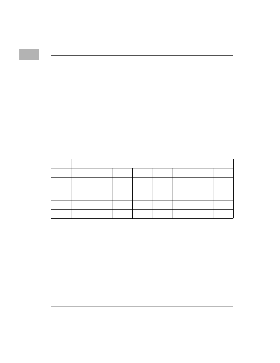
CPU Control Register
The CPU Control register is accessed via the RD[32:39] data lines of the
upper Falcon device. This 8-bit register is defined as follows:
LEMODE Little Endian Mode. This bit must be set in conjunction
with the LEND bit in the Raven for little-endian mode.
P0_TBEN Processor 0 Time Base Enable. When this bit is cleared,
the TBEN pin of the processor will be driven low.
REG
CPU Control Register - $FEF88300
BIT
0
1
2
3
4
5
6
7
FIELD
LEM
O
D
E
P0
_
T
BE
N
OPER
R
R
R
R/W
R
R
R
R
RESET
1
0
0
1
X
X
X
X