Motorola MVME2300 Series User Manual
Page 236
4-12
Computer Group Literature Center Web Site
Universe (VMEbus to PCI) Chip
4
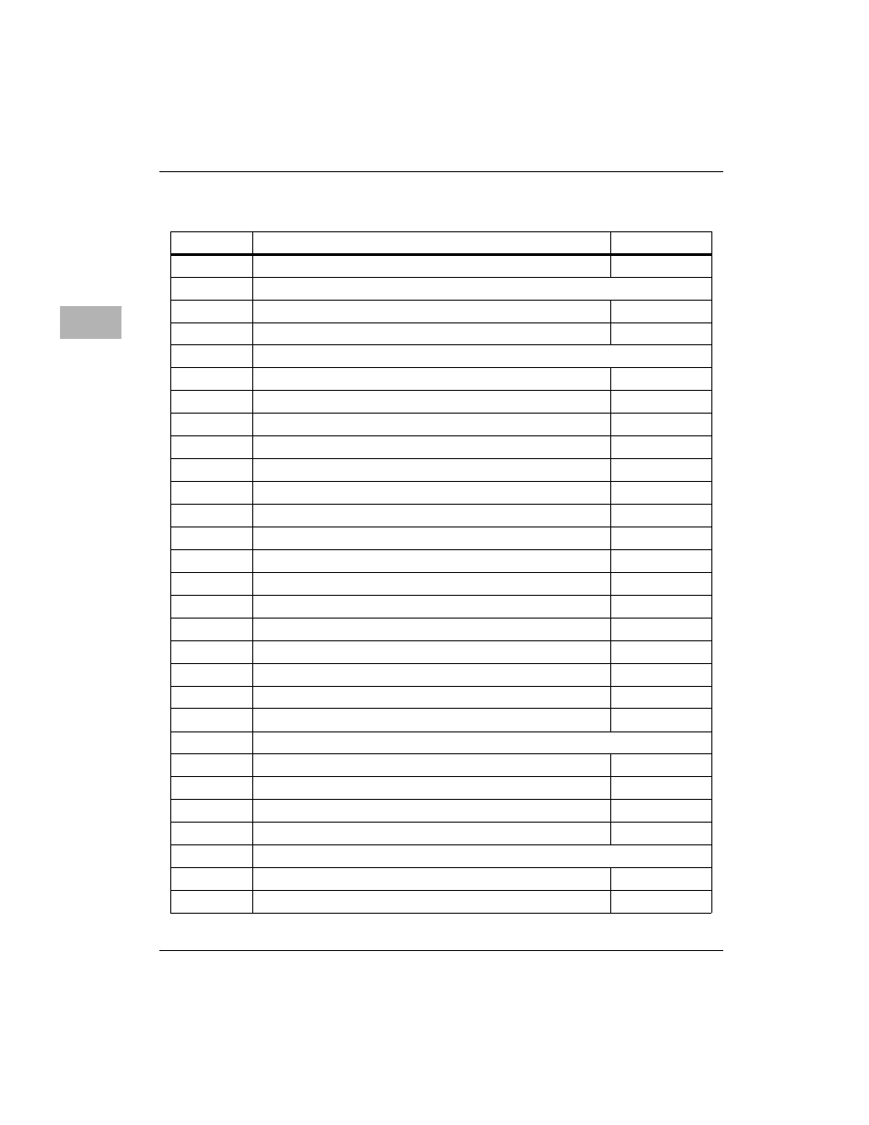
218
DMA Command Packet Pointer
DCPP
21C
Universe Reserved
220
DMA General Control and Status Register
DGCS
224
DMA Linked List Update Enable Register
D_LLUE
228 - 2FC
Universe Reserved
300
PCI Interrupt Enable
LINT_EN
304
PCI Interrupt Status
LINT_STAT
308
PCI Interrupt Map 0
LINT_MAP0
30C
PCI Interrupt Map 1
LINT_MAP1
310
VMEbus Interrupt Enable
VINT_EN
314
VMEbus Interrupt Status
VINT_STAT
318
VMEbus Interrupt Map 0
VINT_MAP0
31C
VMEbus Interrupt Map 1
VINT_MAP1
320
Interrupt Status/ID Out
STATID
324
VIRQ1 STATUS/ID
V1_STATID
328
VIRQ2 STATUS/ID
V2_STATID
32C
VIRQ3 STATUS/ID
V3_STATID
330
VIRQ4 STATUS/ID
V4_STATID
334
VIRQ5 STATUS/ID
V5_STATID
338
VIRQ6 STATUS/ID
V6_STATID
33C
VIRQ7 STATUS/ID
V7_STATID
340 - 3FC
Universe Reserved
400
Master Control
MAST_CTL
404
Miscellaneous Control
MISC_CTL
408
Miscellaneous Status
MISC_STAT
40C
User AM Codes Register
USER_AM
410 - EFC
Universe Reserved
F00
VMEbus Slave Image 0 Control
VSI0_CTL
F04
VMEbus Slave Image 0 Base Address Register
VSI0_BS
Table 4-2. Universe Register Map (Continued)
Offset
Register
Name