Dram attributes register, Dram attributes register -33, Dram – Motorola MVME2300 Series User Manual
Page 195: Attributes register
Programming Model
http://www.motorola.com/computer/literature
3-33
3
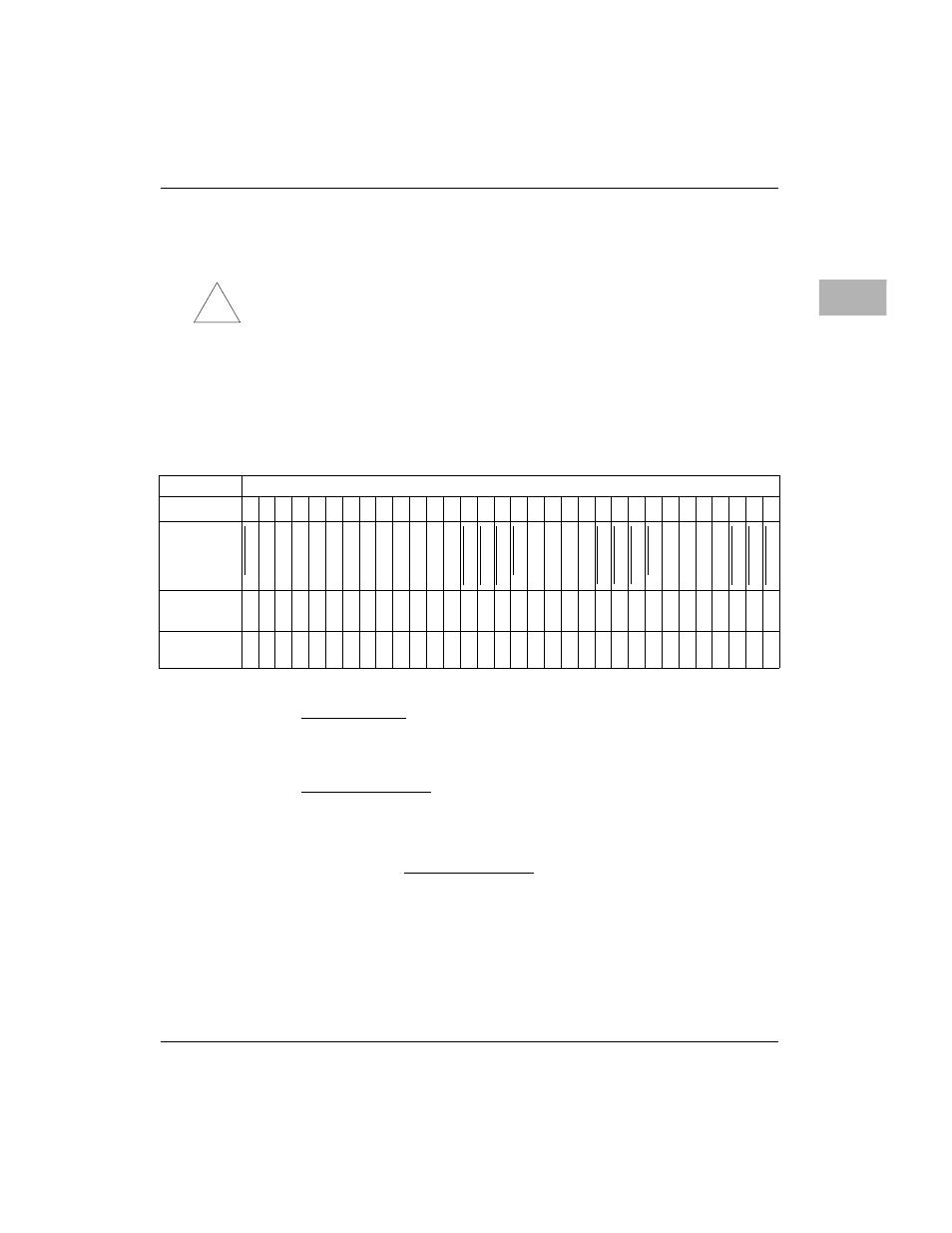
DRAM Attributes Register
!
Caution
To satisfy DRAM component requirements before the memory is used at
start-up, software must always wait at least 500
µ
s after the initial setting
of a bank’s size bits to a nonzero value before the initial access to that
bank. These settings are stored in the DRAM Attributes register (offset
$FEF80010). The delay is introduced to ensure that the bank has been
refreshed at least eight times before use. The 500
µ
s interval is sufficient,
as the CLK Frequency register (offset $FEF80020) is within a factor of
two of matching the actual processor clock frequency.
ram a/b/c/d en
Control bits that enable accesses to the corresponding
block of DRAM when set, and disable them when cleared.
ram a/b/c/d siz0-2
These control bits define the size of their corresponding
block of DRAM.
shows the block
configuration assumed by the Falcon pair for each value
of ram siz0-ram siz2.
ADDRESS
$FEF80010
BIT
0
1
2
3
4
5
6
7
8
9
10
11
12
13
14
15
16
17
18
19
20
21
22
23
24
25
26
27
28
29
30
31
NAME
ra
m a
e
n
0
0
0
0
ra
m a
si
z
0
ra
m a
si
z
1
ra
m a
si
z
2
ra
m b
en
0
0
0
0
ra
m b
siz0
ra
m b
siz1
ra
m b
siz2
ra
m c
e
n
0
0
0
0
ra
m c
si
z
0
ra
m c
si
z
1
ra
m c
si
z
2
ra
m d
en
0
0
0
0
ra
m d
siz0
ra
m d
siz1
ra
m d
siz2
OPERATI
ON
R/W
R
R
R
R
R/W
R/W
R/W
R/W
R
R
R
R
R/W
R/W
R/W
R/W
R
R
R
R
R/W
R/W
R/W
R/W
R
R
R
R
R/W
R/W
R/W
RESET
0 PL
X
X
X
X
0 P
0 P
0 P
0 PL
X
X
X
X
0 P
0 P
0 P
0 PL
X
X
X
X
0 P
0 P
0 P
0 PL
X
X
X
X
0 P
0 P
0 P