Memory configuration register (memcr), Memory configuration register (memcr) -27 – Motorola MVME2300 Series User Manual
Page 51
Programming Model
http://www.motorola.com/computer/literature
1-27
1
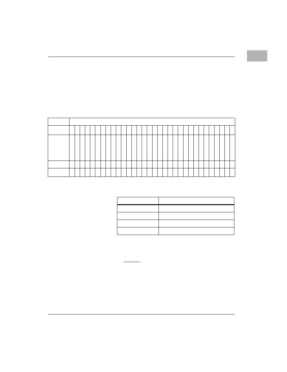
Memory Configuration Register (MEMCR)
The states of the RD[00:31] DRAM data pins, which have weak internal
pull-ups, are latched by the lower Falcon chip at a rising edge of the power-
up reset and stored in this Memory Configuration register to provide some
information about the system memory. Configuration is accomplished
with external pull-down resistors. This 32-bit read-only register is defined
as follows:
M_SIZE[0:1]
Memory Size. This field is encoded as follows:
M_FREF Block A/B/C/D Fast Refresh. When this bit is set, it
indicates that a DRAM block requires faster refresh rate.
If any of the four blocks requires faster refresh rate then
the ram ref control bit should be set.
REG
Memory Configuration Register - $FEF80404
BIT
32
33
34
35
36
37
38
39
40
41
42
43
44
45
46
47
48
49
50
51
52
53
54
55
56
57
58
59
60
61
62
63
FIELD
M_
SIZ
E
0
M_
SIZ
E
1
M_
FR
E
F
M_
SP
D
0
M_
SP
D
1
R_
A_
T
Y
P0
R_
A_
T
Y
P1
R_
A_
T
Y
P2
R_
B_
TYP0
R_
B_
TYP1
R_
B_
TYP2
L2
_TYP
E0
L2
_TYP
E1
L2
_T
Y
P
2
L3
_TYP
E3
L2
_P
LL0
L2
_P
LL1
L2
_P
LL2
L2
_P
LL3
FL
SH
P0
_
FL
SH
P1
_
FLS
H
P2
-
OPER
RESET
X
X
1
X
1
1
X
X
1
X
X
X
1
X
X
X
X
X
X
X
X
X
X
X
1
1
X
X
X
1
1
1
M_SIZE[0:1]
Total Memory On Board
0B00
16 Megabytes
0B01
32 Megabytes
0B10
64 Megabytes
0B11
128 Megabytes