Block diagram of port 0 pins, Port 0 register – FUJITSU Semiconductor Controller MB89950/950A User Manual
Page 87
73
CHAPTER 4 I/O PORTS
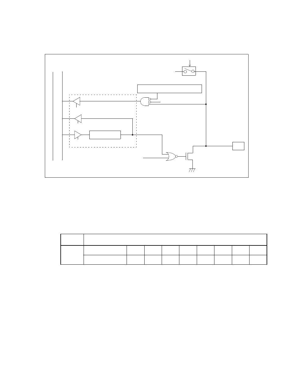
■ Block diagram of port 0 pins
Figure 4.2-1 Block diagram of port 0 pins
■ Port 0 register
The port 0 register consists of PDR0. Each bit in the register has a one-to-one relationship with a port 0 pin.
Table 4.2-2 "Correspondence between pin and register for port 0" shows the correspondence between the
pins and register for port 0.
PDR (Port data register)
In
te
rnal
dat
a
bus
PDR read (for bit manipulation instructions)
Output latch
PDR write
Pin
N-ch
Stop mode (SPL = 1)
SPL: Pin state specification bit in the standby control register (STBC)
PDR read
Stop mode (SPL = 1)
LCD segment driver output
Mask option
Segment driver output select register
Table 4.2-2 Correspondence between pin and register for Port 0
Port
Correspondence between register bit and pin
Port 0
PDR0
Bit 7
Bit 6
Bit 5
Bit 4
Bit 3
Bit 2
Bit 1
Bit 0
Corresponding pin
P07
P06
P05
P04
P03
P02
P01
P00