4 standby control register (stbc), Standby control register (stbc) – FUJITSU Semiconductor Controller MB89950/950A User Manual
Page 75
61
CHAPTER 3 CPU
3.7.4
Standby Control Register (STBC)
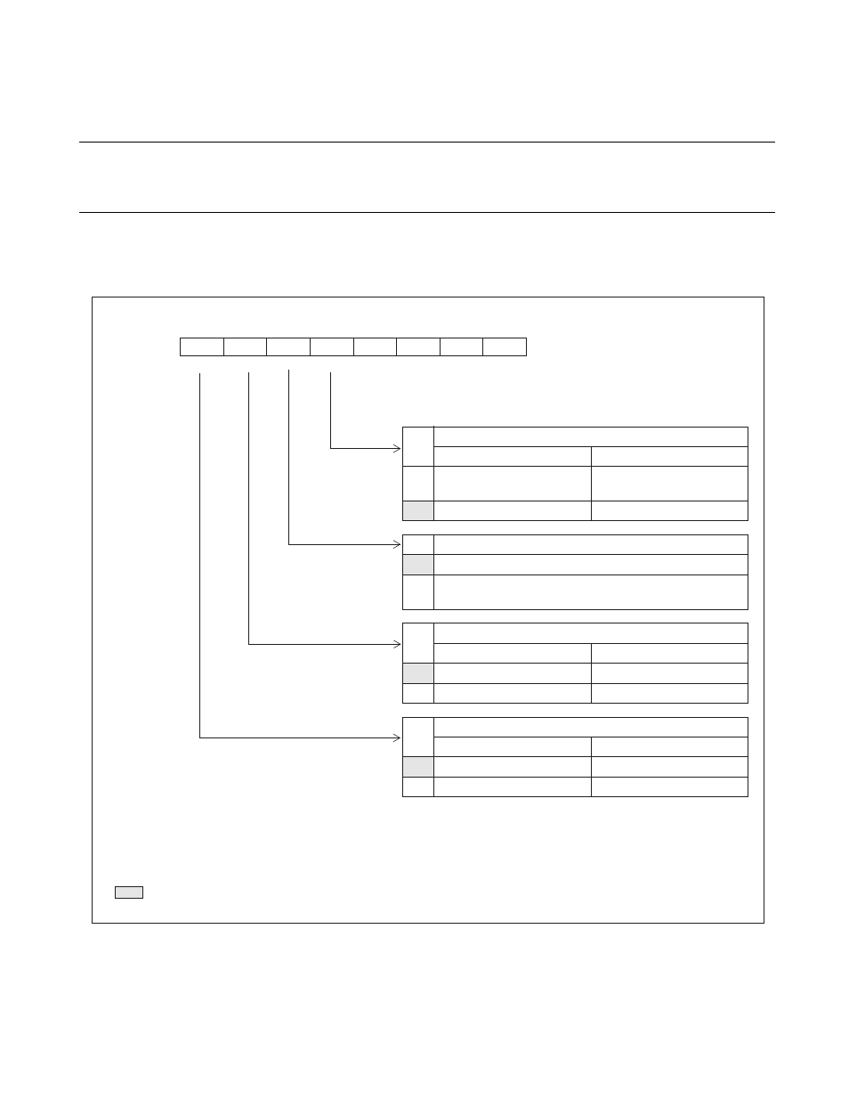
The standby control register (STBC) controls the CPU to enter to sleep mode, stop
mode, sets the pin states in stop mode, and initiates software reset.
■ Standby control register (STBC)
Figure 3.7-1 Standby control register (STBC)
Address
Bit 7
Bit 6
Bit 5
Bit 4
Bit 3
Bit 2
Bit 1
Bit 0
Initial value
0008
H
STP
SLP
SPL
RST
—
—
—
—
0001----
B
W
W
R/W
W
RST
Software reset bi t
Read
Wri te
0
—
Generates a reset signal for
four instruction cycles.
1
Reading always returns “1”.
No effect on operation.
SPL
Pin state specification b it
0
External pins hold their states prior to entering stop mode.
1
External pins go to high-impedance state on entering stop
SLP
Sleep b it
Read
Wri te
0
Reading always returns “0”.
No effect on operation.
1
—
Goes to sleep mode.
STP
Stop bit
Read
Wri te
0
Reading always returns “0”.
No effect on operation.
1
—
Goes to stop mode.
R/W : Readable and writable
W
: Write-only
—
: Unused
X
: Indeterminate
: Initial value
mode.