2 block diagram of pulse width count timer, Block diagram of pulse width count timer – FUJITSU Semiconductor Controller MB89950/950A User Manual
Page 158
144
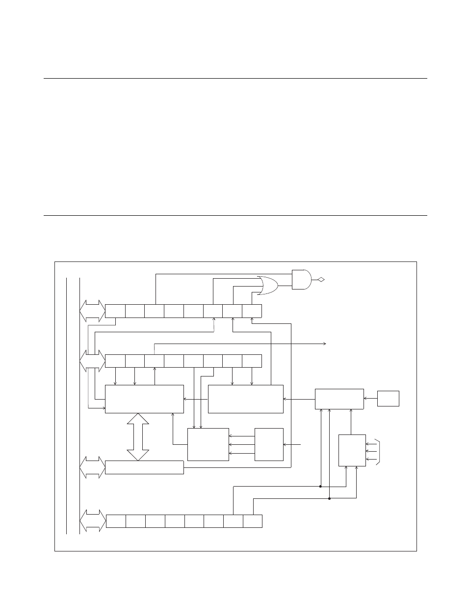
CHAPTER 8 PULSE WIDTH COUNT TIMER (PWC)
8.2
Block Diagram of Pulse Width Count Timer
The pulse width count timer consists of the following nine blocks:
• Count clock selector
• 8-bit down counter
• Input pulse edge detector
• Noise filter circuit
• Noise filter clock selector
• PWC reload buffer register (RLBR)
• PWC pulse width control register 1 (PCR1)
• PWC pulse width control register 2 (PCR2)
• Noise filter control register (NCCR)
■ Block diagram of pulse width count timer
Figure 8.2-1 Block diagram of pulse width count timer
FC
RM
TO
—
C1
C0
W1
W0
Pin
PCR1
PCR2
IRQ3
P42/PWC/INT1
RLBR
X1
X4
X32
EN
—
IE
—
—
UF
IR
BF
1 t
inst
In
te
rnal
dat
a bus
8-bit down counter
Input pulse edge
detector
Count
clock
selector
To PWM timer
Noise filter
—
—
—
—
—
—
NCS1 NCS0
filter
From
timebase
timer
circuit
clock
selector
NCCR
Noise
t
inst
: Instruction cycle