FUJITSU Semiconductor Controller MB89950/950A User Manual
Page 267
253
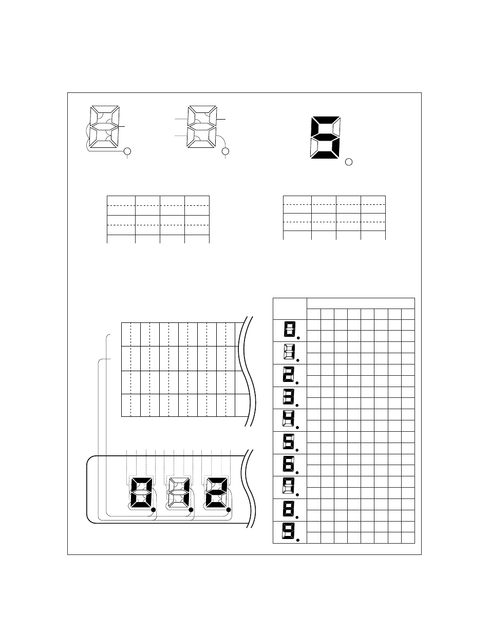
CHAPTER 12 LCD CONTROLLER/DRIVER
●
LCD panel connections and display data example (1/2 duty ratio drive mode)
Figure 12.4-3 Segment/common connections, data states and corresponding display
COM1
COM0
SEG
n+3
SEG
n+2
SEG
n+1
SEG
n
*
7
*
0
*
5
*
4
*
2
*
6
*
1
*
3
SEG0
SEG1
SEG2
SEG3
SEG4
SEG5
SEG6
SEG7
SEG8
SEG9
SEG10
SEG11
COM3
––
––
––
––
––
––
––
––
––
––
––
––
COM2
––
––
––
––
––
––
––
––
––
––
––
––
COM1
0
1
1
1
0
0
1
1
1
1
0
1
COM0
1
1
1
1
0
0
1
0
0
1
1
1
064
H
065
H
066
H
067
H
068
H
069
H
LCD Panel
Display RAM
Address
Segment No.
*0 to *7: I
ndicate corresponding display RAM bits. (Bits 2, 3, 6, and
7 are not used.)
Address
COM3
COM2
COM1
COM0
nH
bit3
bit2
bit1
*1
bit0
*0
SEGn
bit7
bit6
bit5
*3
bit4
*2
SEGn+1
n+1H
bit3
bit2
bit1
*5
bit0
*4
SEGn+2
bit7
bit6
bit5
*7
bit4
*6
SEGn+3
0: OFF
1: ON
Address
COM3
COM2
COM1
COM0
064H
—
—
1
1
SEG0
—
—
1
0
SEG1
065H
—
—
1
0
SEG2
—
—
0
1
SEG3
LCD
Display
Bit States for Numerals "0" through "9"
bit7 bit6 bit5 bit4 bit3 bit2 bit1 bit0
—
—
1
1
—
—
0
1
—
—
1
1
—
—
1
1
—
—
0
0
—
—
0
0
—
—
1
0
—
—
1
1
—
—
1
1
—
—
1
0
—
—
1
1
—
—
0
1
—
—
1
1
—
—
1
0
—
—
1
1
—
—
1
1
—
—
0
0
—
—
1
1
—
—
1
0
—
—
1
1
—
—
1
0
—
—
1
1
—
—
0
1
—
—
1
1
—
—
1
1
—
—
1
1
—
—
0
1
—
—
1
1
—
—
0
0
—
—
0
1
—
—
1
1
—
—
1
1
—
—
1
1
—
—
1
1
—
—
1
1
—
—
1
1
—
—
1
0
—
—
1
1
—
—
1
1
—
—
1
1
Example) Using segments to represent "5".