3 display ram – FUJITSU Semiconductor Controller MB89950/950A User Manual
Page 262
248
CHAPTER 12 LCD CONTROLLER/DRIVER
12.3.3
Display RAM
Display RAM consists of 42 x 4-bit (21 bytes) of display data memory used to generate
the segment output signals.
■ Display RAM and output pins
The contents of display RAM are automatically read out and output via the segment outputs in synchronous
with the selected common signal timing. A "1" bit is converted to a "select" (display on) voltage and a "0"
to a "deselect" (display off) voltage. Since the operation of the LCD is not directly related to the operation
of the CPU, display RAM read/write timing can be set by the user. The SEG20 to SEG41 pins that are not
made dedicated segment outputs by mask option selection may be used as N-ch open-drain I/O port pins,
and the RAM that goes with those pins may be used as regular RAM. (See Table 12.3-3 "Segment outputs,
display RAM locations, and sharing port pins".)
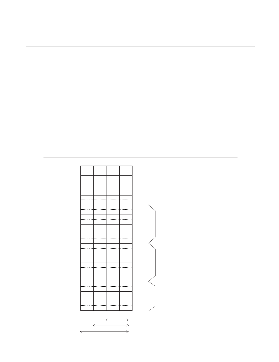
Figure 12.3-7 "Segment/common output pins and corresponding display RAM" shows which display RAM
bits are associated with each segment and common output pin.
Figure 12.3-7 Segment/common output pins and corresponding display RAM
Address
0064
H
bit3
bit2
bit1
bit0
SEG0
bit7
bit6
bit5
bit4
SEG1
0065
H
bit3
bit2
bit1
bit0
SEG2
bit7
bit6
bit5
bit4
SEG3
:
:
:
:
:
:
:
:
:
:
:
:
006D
H
bit3
bit2
bit1
bit0
SEG18
bit7
bit6
bit5
bit4
SEG19
006E
H
bit3
bit2
bit1
bit0
SEG20
bit7
bit6
bit5
bit4
SEG21
006F
H
bit3
bit2
bit1
bit0
SEG22
bit7
bit6
bit5
bit4
SEG23
0070
H
bit3
bit2
bit1
bit0
SEG24
bit7
bit6
bit5
bit4
SEG25
0071
H
bit3
bit2
bit1
bit0
SEG26
bit7
bit6
bit5
bit4
SEG27
0072
H
bit3
bit2
bit1
bit0
SEG28
bit7
bit6
bit5
bit4
SEG29
0073
H
bit3
bit2
bit1
bit0
SEG30
bit7
bit6
bit5
bit4
SEG31
0074
H
bit3
bit2
bit1
bit0
SEG32
bit7
bit6
bit5
bit4
SEG33
0075
H
bit3
bit2
bit1
bit0
SEG34
bit7
bit6
bit5
bit4
SEG35
0076
H
bit3
bit2
bit1
bit0
SEG36
bit7
bit6
bit5
bit4
SEG37
0077
H
bit3
bit2
bit1
bit0
SEG38
bit7
bit6
bit5
bit4
SEG39
0078
H
bit3
bit2
bit1
bit0
SEG40
bit7
bit6
bit5
bit4
SEG41
COM3 COM2 COM1 COM0
Pins SEG36 to SEG41 share pins
with Port 2 (P20 to P25).
RAM area and common pins used in 1/2 duty ratio mode
RAM area and common pins used in 1/3 duty ratio mode
RAM area and common pins used in 1/4 duty ratio mode
Pins SEG28 to SEG35 share pins
with Port 1 (P10 to P17).
Pins SEG20 to SEG27 share pins
with Port 0 (P00 to P07).