Block diagram of uart pins – FUJITSU Semiconductor Controller MB89950/950A User Manual
Page 217
203
CHAPTER 10 UART
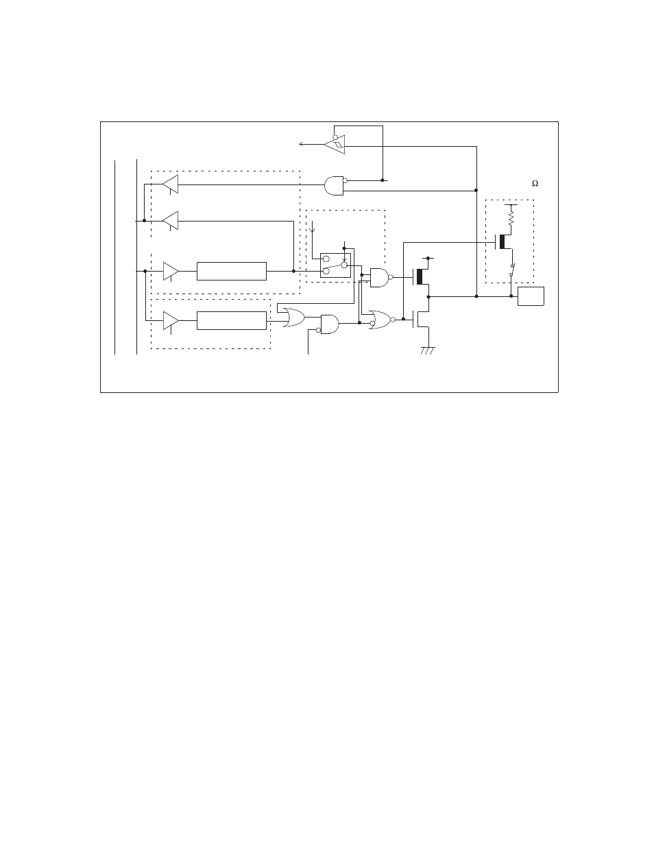
■ Block diagram of UART pins
Figure 10.3-1 Block diagram of UART pins
Reference:
Pins with a pull-up resistor go to the "H" level (pull-up state) rather than to the high-impedance state
when the output transistor is turned "OFF".
PDR (Port data register)
DDR
In
te
rnal
data bus
PDR read
PDR read
Output latch
PDR write
DDR write
Pin
SPL: Pin state specification bit in the standby control register (STBC)
N-ch
Stop mode (SPL = 1)
To peripheral input
(Port data direction register)
UART output
UART
output enable
P-ch
Pull-up resistor
Approx. 50 k
P-ch
(When Read-modify-write instruction executed)
Stop mode (SPL = 1)
(Mask option)
P45/SCK
P44/SO
P43/SI
For P45/SCK and
For P45/SCK and P43/SI
P44/SO