FUJITSU Semiconductor Controller MB89950/950A User Manual
Page 212
198
CHAPTER 10 UART
Figure 10.1-3 Sample calculation of the baud rate (PWM timer is selected)
Refer to CHAPTER 7 "8-BIT PWM TIMER" section for information on the count clock cycle of the PWM
timer, PWM compare register setting value and output cycle of the PWM timer.
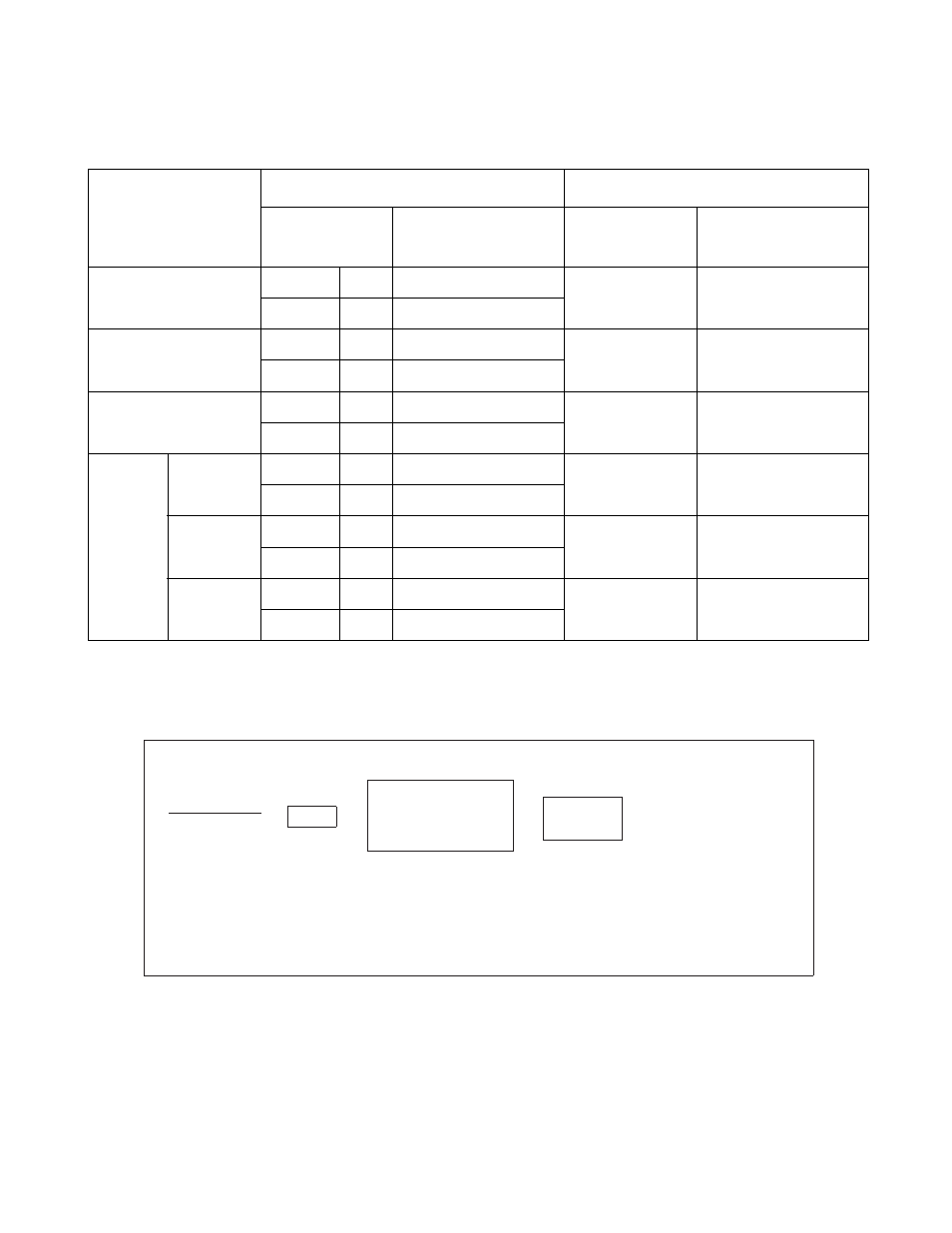
Table 10.1-6 Transfer cycle and transfer rate by 8-bit PWM timers
PWM timer count
clock cycle
Asynchronous transfer mode
Synchronous transfer mode
Clock division
value
Transfer rate
(baud)
(*1)
Clock division
value
Transfer rate
(baud)
(*1)
1 t
inst
CR = 0
16
39062 to 152.6
2
312.5k to 1.22k
CR = 1
64
9765.6 to 38.1
16 t
inst
CR = 0
16
2441.4 to 9.5
2
19531.3 to 76.3
CR = 1
64
610.4 to 2.4
64 t
inst
CR = 0
16
610.4 to 2.4
2
4882.8 to 19.1
CR = 1
64
152.6 to 0.6
From
PWC
timer
1 t
inst
CR = 0
16
19531.3 to 76.3
2
156.3 to 610.4
CR = 1
64
4882.8 to 19.1
4 t
inst
CR = 0
16
4882.8 to 19.1
2
39062 to 152.6
CR = 1
64
1220.7 to 4.8
32 t
inst
CR = 0
16
610.4 to 2.38
2
4882.8 to 19.1
CR = 1
64
152.3 to 0.6
t
inst
: Instruction cycle
*1: Main clock oscillation frequency (F
CH
) = 5 MHz
1
Baud rate value
Clock
selection
4/F
CH
=
X
Compare
register
value+1
Compare register
(COMR)
X
X 2 X CR
(
CR = 0 ..16
)
CR = 1 .. 64
(Cycle time)
1 (P1 = 0, P0 = 0)
16 (P1 = 0, P0 = 1)
32 (P1 = 1, P0 = 0)
PWC (P1 = 1, P0 = 1)*
Input clock select bits
(PWM timer)
*
: PWC value depends on the value of PWC pulse width control register 2, bit 3 and bit 2 (PCR2:C1, C0).
C1=0, C0=0 -> 1
C1=0, C0=1 -> 4
C1=1, C0=0 -> 32
C1=1, C0=1 -> Prohibited
F
CH
: Main clock oscillation frequency