V1 to v3 pin voltages, Difference in potential between com0 and, Difference in potential between com1 and – FUJITSU Semiconductor Controller MB89950/950A User Manual
Page 269: Difference in potential between com2 and, Difference in potential between com0 and seg, Difference in potential between com1 and seg, Difference in potential between com2 and seg, 1 frame 1 cycle
255
CHAPTER 12 LCD CONTROLLER/DRIVER
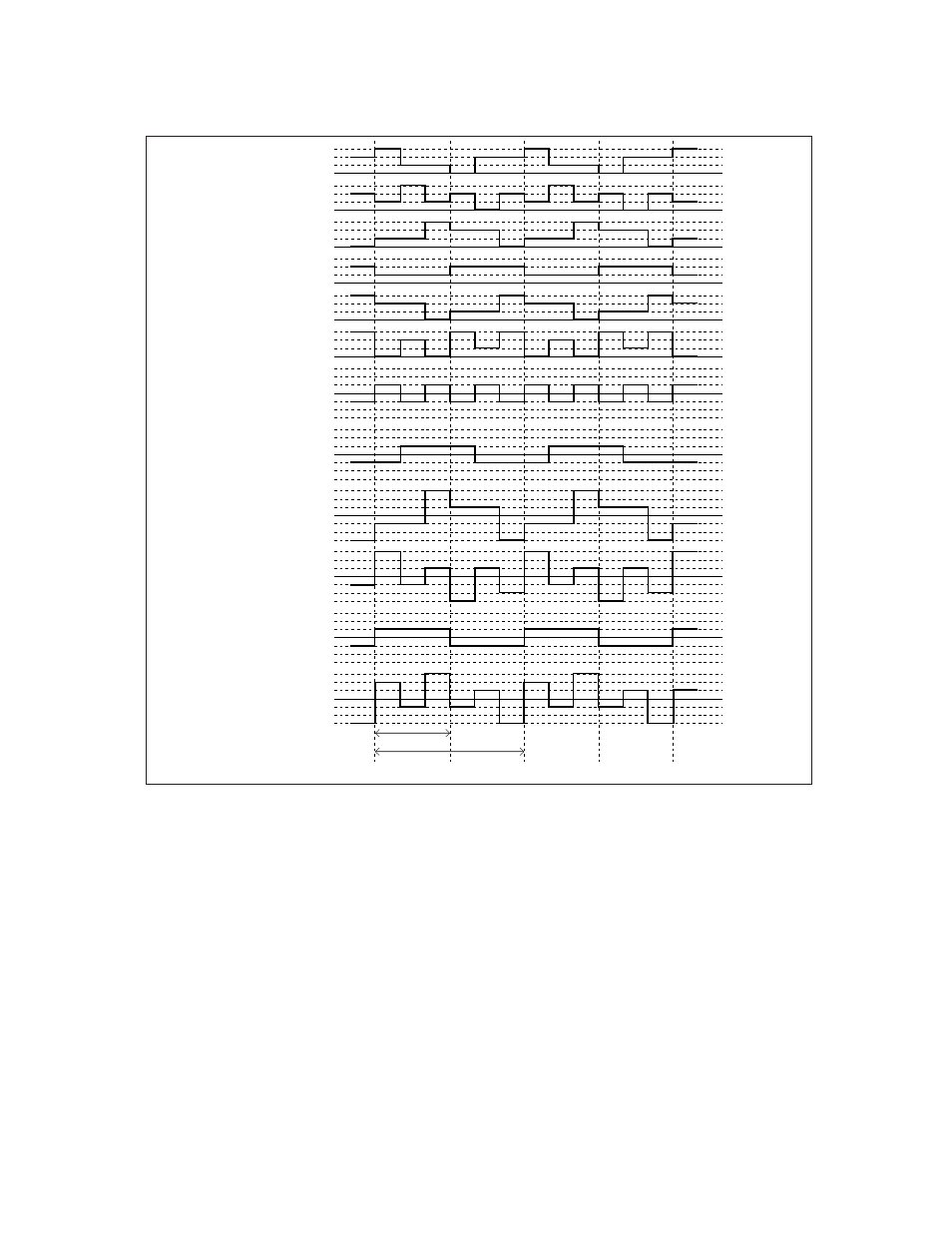
Figure 12.4-4 Output waveforms, 1/3 bias and 1/3 duty ratio example
V
3
V
2
V
1
V
0
=V
SS
V
3
V
2
V
1
V
0
=V
SS
V
3
V
2
V
1
V
0
=V
SS
V
3
V
2
V
1
V
0
=V
SS
V
3
V
2
V
1
V
0
=V
SS
V
3
V
2
V
1
V
0
=V
SS
V
3
(ON)
V
2
V
1
V
SS
-V
1
-V
2
-V
3
(ON)
V
3
(ON)
V
2
V
1
V
SS
-V
1
-V
2
-V
3
(ON)
V
3
(ON)
V
2
V
1
V
SS
-V
1
-V
2
-V
3
(ON)
V
3
(ON)
V
2
V
1
V
SS
-V
1
-V
2
-V
3
(ON)
V
3
(ON)
V
2
V
1
V
SS
-V
1
-V
2
-V
3
(ON)
V
3
(ON)
V
2
V
1
V
SS
-V
1
-V
2
-V
3
(ON)
COM0
COM1
COM2
COM3
SEG
n
SEG
n+1
Difference in
potential between
COM0 and
SEG
n
Difference in
potential between
COM1 and
SEG
n
Difference in
potential between
COM2 and
SEG
n
Difference in
potential between
COM0 and SEG
n+1
Difference in
potential between
COM1 and SEG
n+1
Difference in
potential between
COM2 and SEG
n+1
1 frame
1 cycle
V
1
to V
3
: V1 to V3 pin voltages