Block diagram of port 3 pins – FUJITSU Semiconductor Controller MB89950/950A User Manual
Page 101
87
CHAPTER 4 I/O PORTS
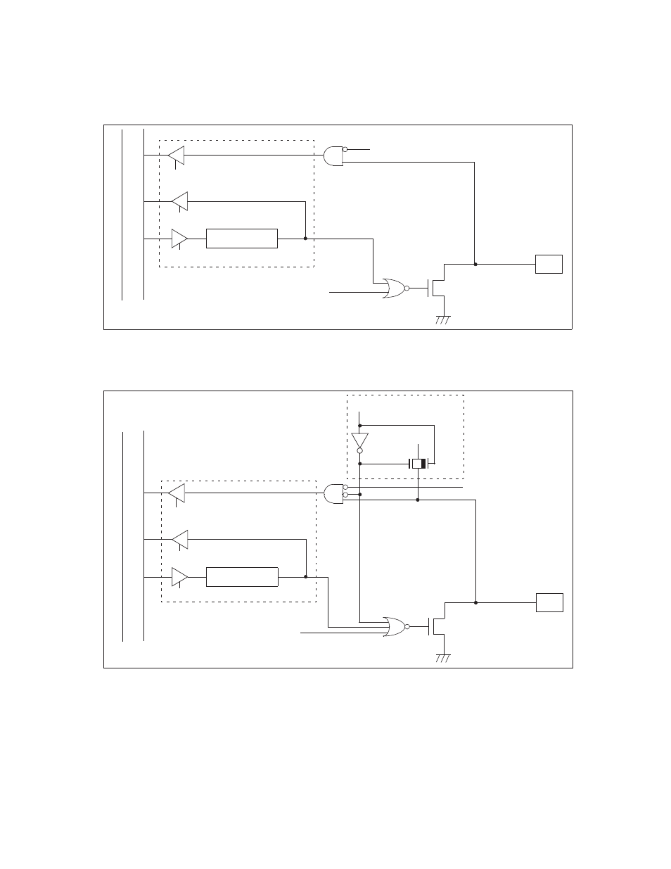
■ Block diagram of port 3 pins
Figure 4.5-1 Block diagram of port 3 pins (P30 and P31)
Figure 4.5-2 Block diagram of port 3 pins (P32/V1 and P33/V2)
PDR (Port data register)
In
te
rnal
dat
a
bus
PDR read (for bit manipulation instructions)
Output latch
PDR write
Pin
N-ch
Stop mode (SPL = 1)
SPL: Pin state specification bit in the standby control register (STBC)
PDR read
Stop mode (SPL = 1)
PDR (Port data register)
In
te
rn
al
dat
a
bus
PDR read (for bit manipulation instructions)
Output latch
PDR write
Pin
N-ch
Stop mode (SPL = 1)
SPL: Pin state specification bit in the standby control register (STBC)
PDR read
Stop mode (SPL = 1)
PSEL bit of LCDR register
V1 or V2
N-ch
P-ch