Description" and table 1.7-2 "pin descr – FUJITSU Semiconductor Controller MB89950/950A User Manual
Page 28
14
CHAPTER 1 OVERVIEW
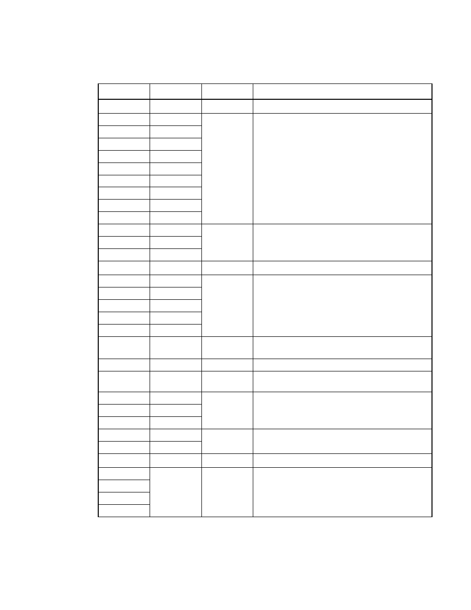
Table 1.7-2 Pin description for external ROM (for MB89PV950 only)
Pin no.
Pin name
I/O
Function
66
V
PP
O
For high-level output.
67
A12
O
For address output.
68
A7
69
A6
70
A5
71
A4
72
A3
73
A2
74
A1
75
A0
77
O1
I
For data input.
78
O2
79
O3
80
V
SS
O
For power supply (GND).
82
O4
I
For data input.
83
O5
84
O6
85
O7
86
O8
87
CE
O
For ROM chip enable.
The High level is output in standby mode.
88
A10
O
For address output.
89
OE
O
For ROM output enable.
The Low level is always output.
91
A11
O
For address output.
92
A9
93
A8
94
A13
O
For address output.
95
A14
96
V
CC
O
For EPROM power supply.
65
N.C.
--
For internal connection.
Keep open.
76
81
90