2 block diagram of timebase timer, Block diagram of timebase timer – FUJITSU Semiconductor Controller MB89950/950A User Manual
Page 116
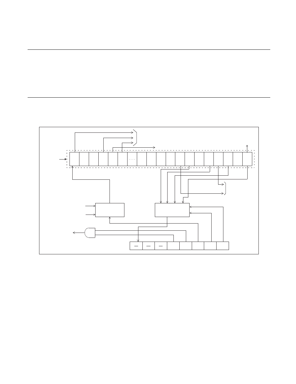
102
CHAPTER 5 TIMEBASE TIMER
5.2
Block Diagram of Timebase Timer
The timebase timer consists of the following four blocks:
• Timebase timer counter
• Counter clear circuit
• Interval timer selector
• Timebase timer control register (TBTC)
■ Block diagram of timebase timer
Figure 5.2-1 Block diagram of timebase timer
●
Timebase timer counter
A 20-bit up counter that uses the divide-by-two main clock oscillation frequency as a count clock. The
counter stops when the main clock oscillator is stopped.
●
Counter clear circuit
In addition to being cleared by setting the TBTC register (TBR = "0"), the counter is cleared when device
goes to stop mode (STBC: STP = "1") or by power-on reset (optional).
●
Interval timer selector
Selects one of four operating timebase timer counter bits as the interval timer bit. An overflow on the
selected bit triggers an interrupt.
TBTC
OF
OF
OF
Timebase
timer counter
Divide-by
-two F
CH
Power-on reset
Stop mode start
IRQ6
Timebase timer
interrupt
OF: Overflow
Counter
clear circuit
Interval
timer selector
To watchdog timer
To clock controller
for the oscillation
stabilization delay
time selector
1
3
4
5
6
9
10
11
12
13
14
15
16
17
18
19
x 2
x 2
x 2
x 2
x 2
x 2
x 2
x 2
x 2
x 2
x 2
x 2
x 2
x 2
x 2
x 2
2
x 2
x 2
20
OF
Counter clear
TBR TBC1 TBC0
TBIF
TBIE
To PWC
To LCD controller/driver
F
CH
: Main clock oscillation frequency