FUJITSU Semiconductor Controller MB89950/950A User Manual
Page 64
50
CHAPTER 3 CPU
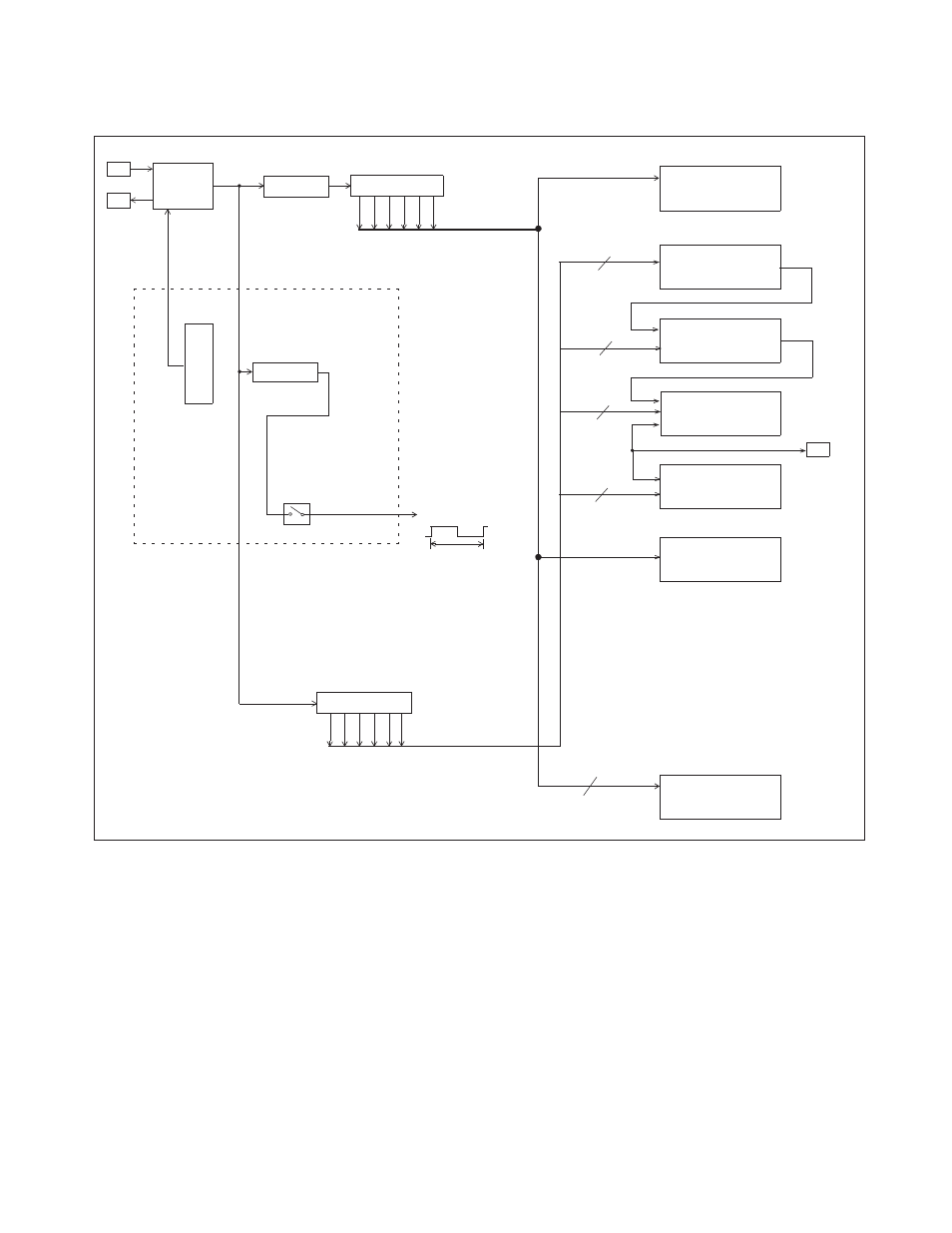
Figure 3.6-1 Clock supply map
LCD controller/driver
Serial I/O
Peripheral functions
Timebase timer
Supply to the CPU
1 t
inst
Clock controller
Pin
X1
Pin
X0
O
s
ci
lla
ti
o
n
Watchdog timer
8-bit PWM timer
UART
Main clock
oscillator
Divide-by-two
F
CH
Oscillation stabilization
delay controller
Pin
SCK
Free-run counter
cont
ro
ll
er
Divide-by-four
Sleep/stop mode
oscillation stabilization delay
F
CH
: Main clock oscillation frequency
t
inst
: Instruction cycle (divide-by-four main clock oscillation)
Clock mode
Stop mode
3
4
2
8-bit PWC timer
3
3