Block diagram of port 4 pins, Port 4 registers – FUJITSU Semiconductor Controller MB89950/950A User Manual
Page 107
93
CHAPTER 4 I/O PORTS
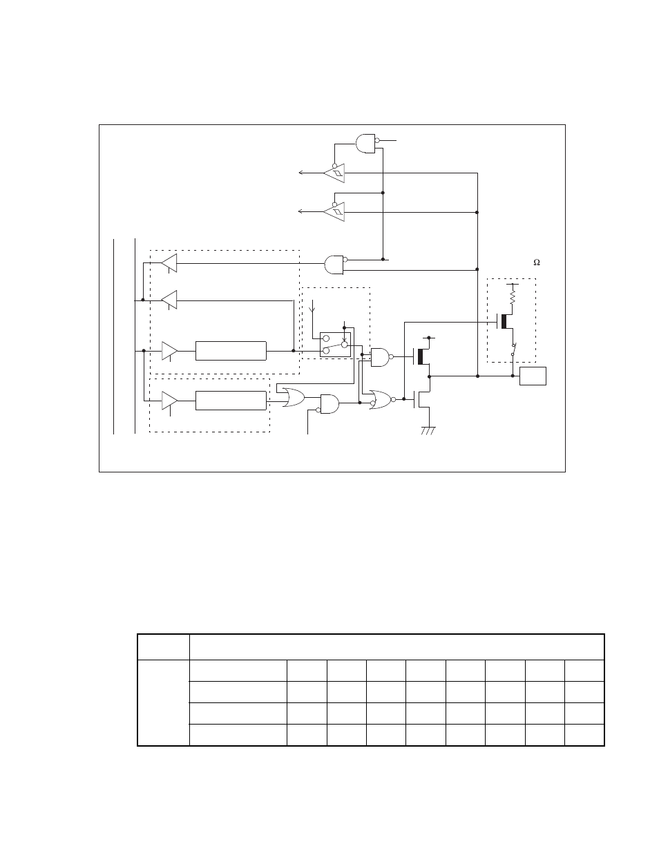
■ Block diagram of port 4 pins
Figure 4.6-1 Block diagram of port 4 pins
Reference:
Peripheral inputs continuously input the pin value (except during stop mode).
■ Port 4 registers
The port 4 registers consist of PDR4 and DDR4.
Each bit in these registers has a one-to-one relationship with a port 4 bit and port 4 pin.
Table 4.6-2 "Correspondence between pin and register for port 4" shows the correspondence between pins
and registers for port 4.
PDR (Port data register)
DDR
In
te
rnal
data bus
PDR read
PDR read
Output latch
PDR write
DDR write
Pin
SPL: Pin state specification bit in the standby control register (STBC)
N-ch
Stop mode (SPL = 1)
To peripheral input
(Port data direction register)
Peripheral output
Peripheral
output enable
P-ch
Pull-up resistor
Approx. 50 k
P-ch
(When Read-modify-write instruction executed)
Stop mode (SPL = 1)
To external interrupt
External interrupt enable
(Mask option)
Table 4.6-2 Correspondence between pin and register for port 4
Port
Correspondence between register bit and pin
Port 4
PDR4
Bit 7
Bit 6
Bit 5
Bit 4
Bit 3
Bit 2
Bit 1
Bit 0
Corresponding pin
--
P46
P45
P44
P43
P42
P41
P40
DDR4
Bit 7
Bit 6
Bit 5
Bit 4
Bit 3
Bit 2
Bit 1
Bit 0
Corresponding pin
--
P46
P45
P44
P43
P42
P41
P40