HEIDENHAIN PT 855 for Turning User Manual
Page 79
II - 6
Switching Inputs and Outputs
POSITIP 855
Technical Information
81
Reset actual value display to zero
You can reset the actual value display of each axis to zero through
one of the inputs at pin 2 to pin 5 (see previous page).
Minimum pulse duration for zero reset: t
min
≥
100 ms
Zero reset signal: make contact against 0 V or
input pulse over TTL logic device (such as SN 74 LS XX):
U
H
≥
3.9 V (U
MAX
= 15 V)
U
L
≤
0.9 V with I
L
≤
6 mA
Using the switching signals
If you wish to use the switching signals, you must supply POSITIP
with 24 V DC at the D-sub connection EXT (pins 23 to 25; 0 V to
pin 10). Pins 14 to 21 will then be supplied with 24 V as long as the
display value is not within a switching range.
These pins are then assigned to the axes with operating parameter
P60.x. As soon as a display value is within the switching range, the
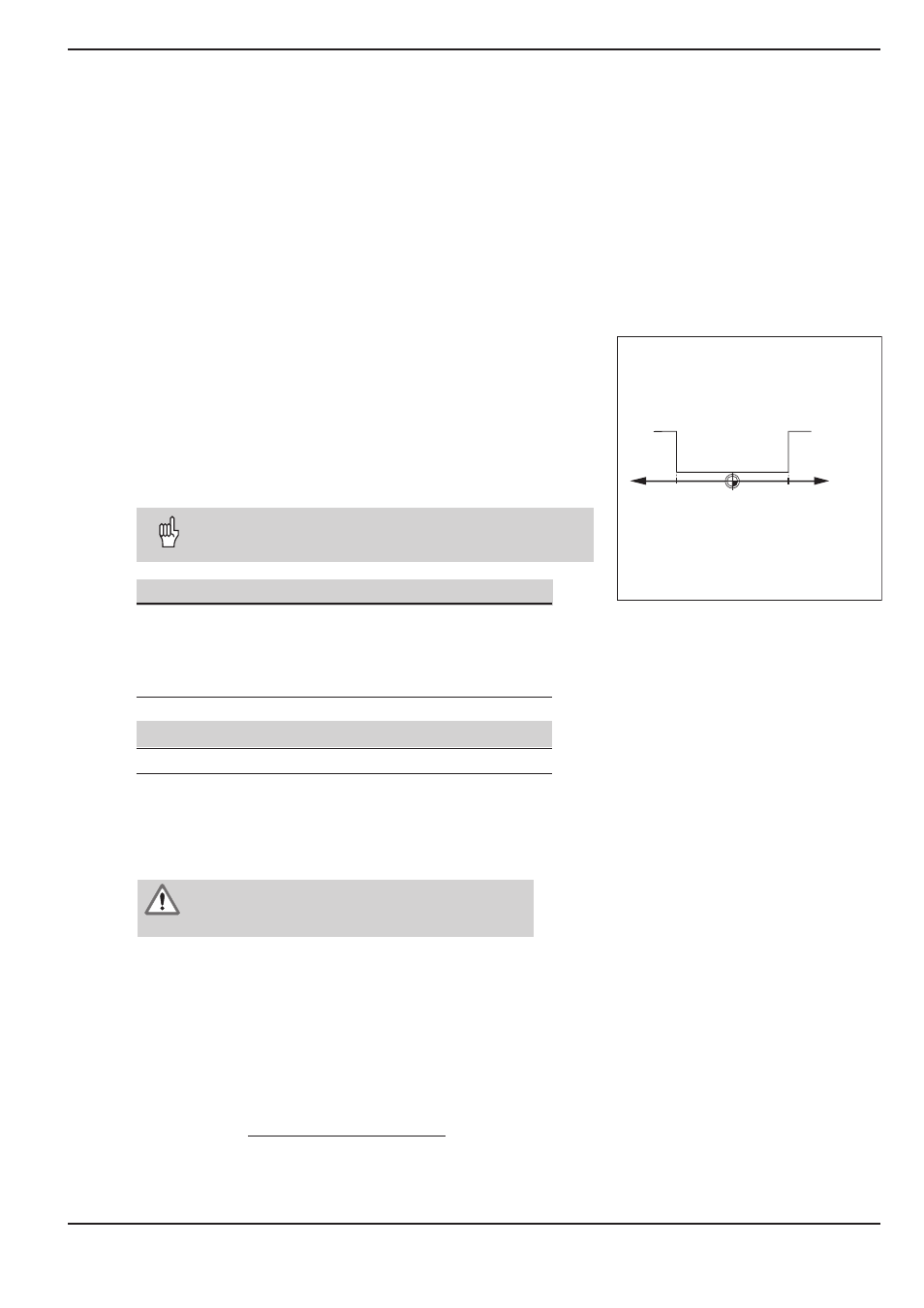
voltage to the corresponding pin will be cut off. Define the switch-
ing range in operating parameter P61.x symmetrically around zero.
If the location of the datum point changes, move the
switching ranges correspondingly.
Axis assignment: P60.x
No axis assigned (Off):
P60.x = 0
Assigned to axis 1:
P60.x = 1
Assigned to axis 2:
P60.x = 2
Assigned to axis 3:
P60.x = 3
Assigned to axis 4:
P60.x = 4
Define the switching range: P 61.x
0 to 99 999.999 [mm] symmetrically around zero
P61.x
Permissible load at switching outputs
I
MAX
= 100 mA
DC resistance
Connect inductive load only with quenching diode.
Accuracy of switching ranges and switching delay: P 69
You can select the switching delay and the accuracy with which
the switching outputs are switched.
You can choose between
•
Accuracy = display step; switching delay = 80 ms
This is mode 1: P 69 = 0
•
Accuracy =
Grating period GP of encoder
Switching delay = 5 ms. This is mode 2: P 69 =1
Danger to internal components!
Connect inductive loads only with a quench-
ing diode parallel to the inductance.
128
P60.2
P61.2
P61.2
X:
0
–
+
Fig. 46: The switching ranges are symmetrical
around zero