Micro sd flash memory, Micro sd flash memory –52 – Altera Arria V SoC Development Board User Manual
Page 60
2–52
Chapter 2: Board Components
Memory
July 2014
Altera Corporation
Reference Manual
Micro SD Flash Memory
The development board supports a micro SD card interface using x4 data lines. The
HPS dedicated interface and the USB 2.0 OTG interface are mutually exclusive since
both interfaces share some pins. The interface selection is done using the DIP switch.
The data and control lines are multiplexed or demultiplexed using on the board’s
analog switches. The micro SD card interface may contain secondary boot code.
This 4-bit data interface can sustain burst read operations at up to 50 MHz for a
throughput of 25 MBps.
lists the micro SD flash memory interface pin assignments, signal names,
and functions. The signal names and types are relative to the Arria V SoC in terms of
I/O setting and direction.
C8
FSM_A21
1.8-V
Address bus
A8
FSM_A22
1.8-V
Address bus
G1
FSM_A23
1.8-V
Address bus
H8
FSM_A24
1.8-V
Address bus
B6
FSM_A25
1.8-V
Address bus
B8
FSM_A26
1.8-V
Address bus
F2
FSM_D0
1.8-V
Data bus
E2
FSM_D1
1.8-V
Data bus
G3
FSM_D2
1.8-V
Data bus
E4
FSM_D3
1.8-V
Data bus
E5
FSM_D4
1.8-V
Data bus
G5
FSM_D5
1.8-V
Data bus
G6
FSM_D6
1.8-V
Data bus
H7
FSM_D7
1.8-V
Data bus
E1
FSM_D8
1.8-V
Data bus
E3
FSM_D9
1.8-V
Data bus
F3
FSM_D10
1.8-V
Data bus
F4
FSM_D11
1.8-V
Data bus
F5
FSM_D12
1.8-V
Data bus
H5
FSM_D13
1.8-V
Data bus
G7
FSM_D14
1.8-V
Data bus
E7
FSM_D15
1.8-V
Data bus
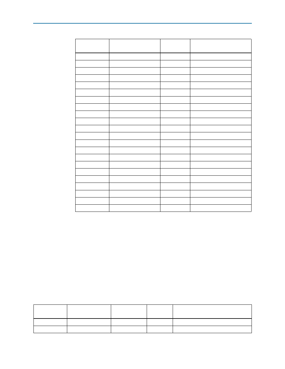
Table 2–31. Flash Pin Assignments, Schematic Signal Names, and Functions (Part 2 of 2)
Board
Reference (U13)
Schematic Signal Name
I/O Standard
Description
Table 2–32. Micro SD Flash Memory Interface Schematic Signal Names and Functions (Part 1 of 2)
Board
Reference (J5)
Schematic Signal
Name
Arria V SoC Pin
Number
I/O Standard
Description
5
SD_CLK
L16
3.3-V Clock
7
SD_DAT0
C17
3.3-V Data
bus