Altera Arria V SoC Development Board User Manual
Page 35
Chapter 2: Board Components
2–27
Components and Interfaces
July 2014
Altera Corporation
Reference Manual
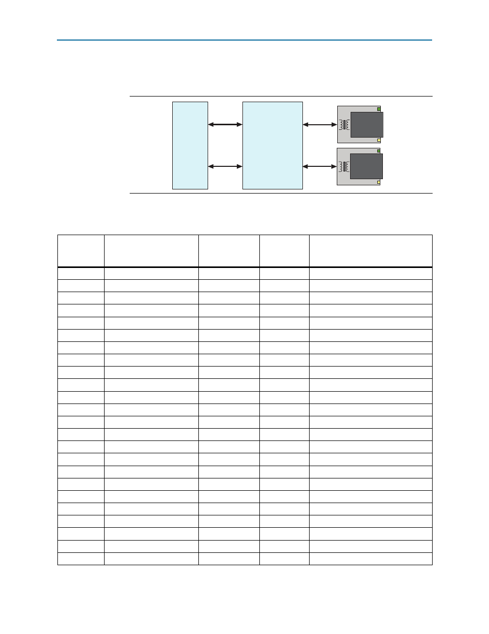
shows the MII interface between the FPGA (MAC) and Renesas uPD60620
PHY.
lists the Ethernet PHY interface pin assignments.
Figure 2–8. MII Interface between FPGA (MAC) and PHY
FPGA MII
Mac
Dual-Port RGMII
Renesas
uPD60620
RJ-45
RJ-45
Table 2–19. Ethernet PHY (FPGA) Pin Assignments, Signal Names and Functions (Part 1 of 2)
Board
Reference
(U55)
Schematic Signal Name
Arria V SoC Pin
Number
I/O Standard
Description
68
ENET1_ACT_LED
—
2.5-V
Receive data active LED
69
ENET1_LINK_LED
—
2.5-V
Transmit data active LED
18
ENET1_MDI_RX_N
—
2.5-V
Media dependent interface
17
ENET1_MDI_RX_P
—
2.5-V
Media dependent interface
16
ENET1_MDI_TX_N
—
2.5-V
Media dependent interface
15
ENET1_MDI_TX_P
—
2.5-V
Media dependent interface
59
ENET1_RX_CLK
AE22
2.5-V
MII receive clock
53
ENET1_RX_D0
AL23
2.5-V
MII receive data bus
54
ENET1_RX_D1
AW22
2.5-V
MII receive data bus
55
ENET1_RX_D2
AW21
2.5-V
MII receive data bus
56
ENET1_RX_D3
AV21
2.5-V
MII receive data bus
57
ENET1_RX_DV
AF22
2.5-V
MII receive data valid
58
ENET1_RX_ERROR
AH23
2.5-V
MII receive error
49
ENET1_TX_CLK_FB
AN23
2.5-V
25-MHz MII transmit clock
43
ENET1_TX_D0
AU22
2.5-V
MII transmit data bus
44
ENET1_TX_D1
AT22
2.5-V
MII transmit data bus
45
ENET1_TX_D2
AE23
2.5-V
MII transmit data bus
46
ENET1_TX_D3
AD22
2.5-V
MII transmit data bus
48
ENET1_TX_EN
AP23
2.5-V
MII transmit enable
65
ENET2_ACT_LED
—
2.5-V
Receive data active LED
67
ENET2_LINK_LED
—
2.5-V
Transmit data active LED
4
ENET2_MDI_RX_N
—
2.5-V
Media dependent interface
5
ENET2_MDI_RX_P
—
2.5-V
Media dependent interface
6
ENET2_MDI_TX_N
—
2.5-V
Media dependent interface