Altera Arria V SoC Development Board User Manual
Page 14
2–6
Chapter 2: Board Components
MAX V CPLD 5M2210 System Controller
July 2014
Altera Corporation
Reference Manual
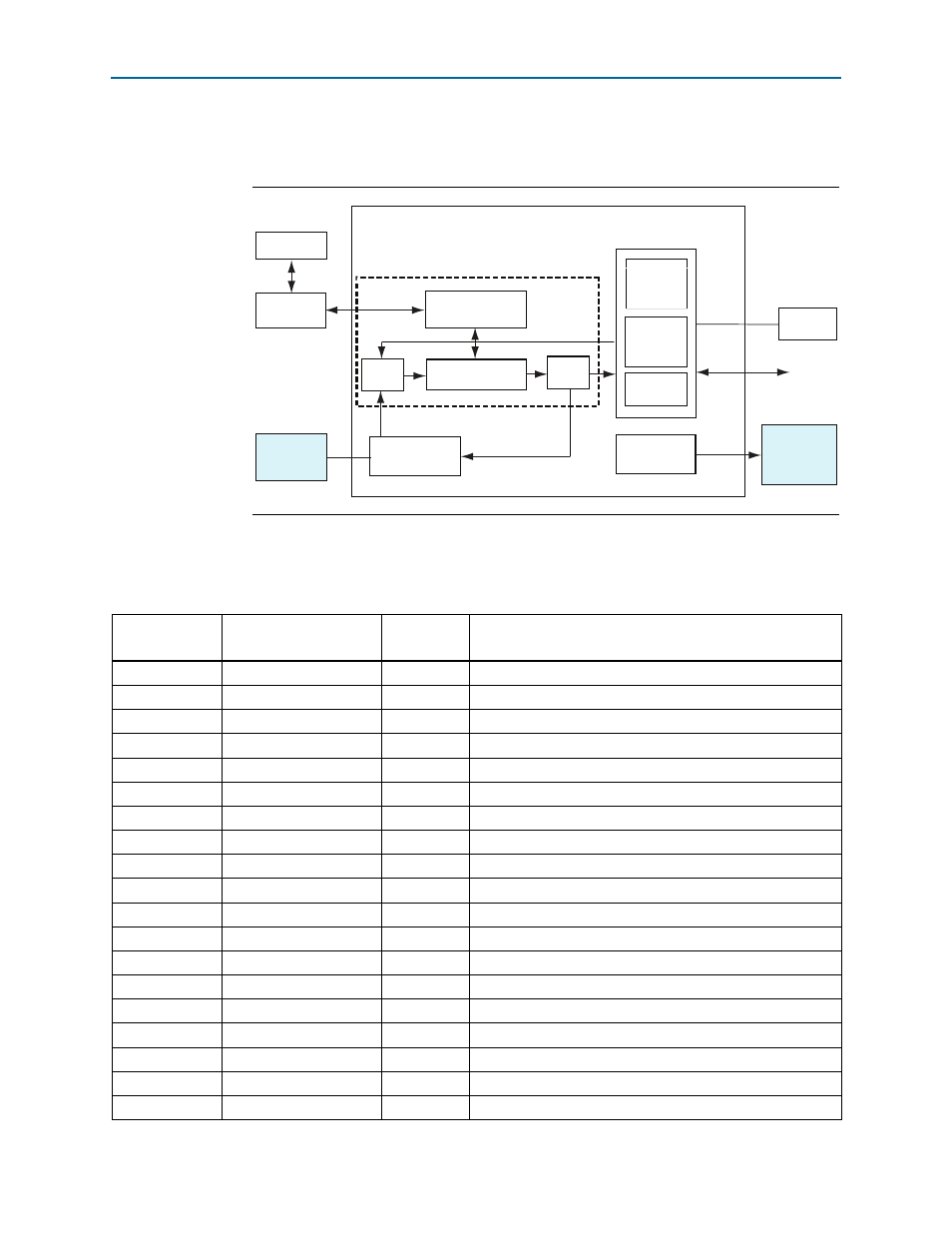
illustrates the MAX V CPLD 5M2210 System Controller's functionality and
external circuit connections as a block diagram.
lists the I/O signals present on the MAX V CPLD System Controller. The
signal names and functions are relative to the MAX V device.
Figure 2–2. MAX V CPLD 5M2210 System Controller Block Diagram
Information
Register
Embedded
USB-Blaster II
Oscillator
Controller
SLD-HUB
PFL
SPI Bus
MAX V CPLD System Controller
LTC 2978
Power
Controllers
Virtual-JTAG
PC
FPGA
I
2
C
Controller
Decoder
Encoder
GPIO
JTAG Control
Control
Register
Si570, Si571,
Si5338
Programmable
Oscillator
Table 2–3. MAX V CPLD System Controller Device Pin-Out (Part 1 of 5)
Board
Reference (U27)
Schematic Signal Name
I/O Standard
Description
B9
CLK125A_EN
2.5-V
125 MHz oscillator enable
E9
CLK50_EN
2.5-V
50 MHz oscillator enable
J5
CLK_100M_MAX
2.5-V
100 MHz clock input
J12
CLK_50M_MAX
1.8-V
50 MHz clock input
D10
CPU_RESETN
2.5-V
FPGA reset push button
N11
EXTRA_SIG0
1.5-V
On-board USB-Blaster II interface. Reserved for future use
T13
EXTRA_SIG1
1.5-V
On-board USB-Blaster II interface. Reserved for future use
T15
EXTRA_SIG2
1.5-V
On-board USB-Blaster II interface. Reserved for future use
A2
FACTORY_LOAD
2.5-V
DIP switch to load factory or user design at power-up
R14
FACTORY_REQUEST
1.5-V
On-board USB-Blaster II request to send FACTORY command
N12
FACTORY_STATUS
1.5-V
On-board USB-Blaster II FACTORY command status
F11
FLASH_ADVN
1.8-V
FSM bus flash memory address valid
N14
FLASH_CEN0
1.8-V
FSM bus flash memory chip enable
D14
FLASH_CLK
1.8-V
FSM bus flash memory clock
P15
FLASH_OEN
1.8-V
FSM bus flash memory output enable
P14
FLASH_RDYBSYN
1.8-V
FSM bus flash memory ready
D13
FLASH_RESETN
1.8-V
FSM bus flash memory reset
N15
FLASH_WEN
1.8-V
FSM bus flash memory write enable
E14
FM_A0
1.8-V
FM address bus