Power supply, Power supply –57 – Altera Stratix IV E FPGA Development Board User Manual
Page 65
Chapter 2: Board Components
2–57
Power Supply
May 2011
Altera Corporation
Stratix IV E FPGA Development Board Reference Manual
lists the flash component reference and manufacturing information.
Power Supply
The development board's power is provided through a laptop style DC power input.
The input voltage must be in the range of 14 V to 20 V. The DC voltage is then stepped
down to various power rails used by the components on the board.
An on-board multi-channel analog-to-digital converter (ADC) is used to measure both
the voltage and current for several specific board rails. The power utilization is
displayed in a GUI that graphs power consumption versus time.
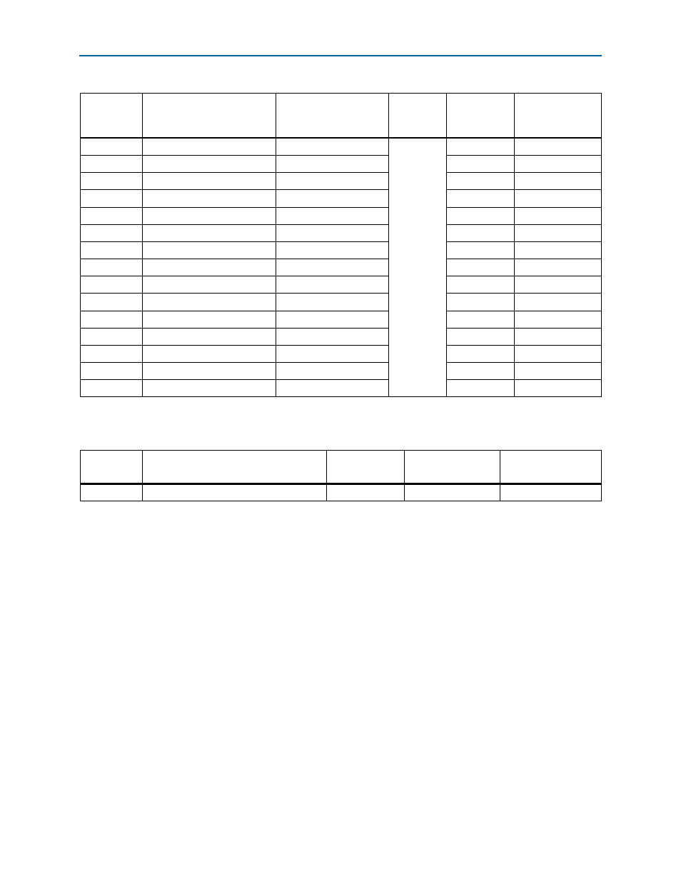
U2.E2
Data bus
FSM_D1
2.5-V
F28
U10.R1, U3.J11
U2.G3
Data bus
FSM_D2
E28
U10.P5, U3.K10
U2.E4
Data bus
FSM_D3
D30
U10.T2, U3.K11
U2.E5
Data bus
FSM_D4
C30
U10.N5, U3.L10
U2.G5
Data bus
FSM_D5
F29
U10.R3, U3.L11
U2.G6
Data bus
FSM_D6
E29
U10.P6, U3.M10
U2.H7
Data bus
FSM_D7
J24
U10.R4, U3.M11
U2.E1
Data bus
FSM_D8
J25
U10.N6, U3.D10
U2.E3
Data bus
FSM_D9
A24
U10.T4, U3.D11
U2.F3
Data bus
FSM_D10
A26
U10.M6, U3.E10
U2.F4
Data bus
FSM_D11
B25
U10.R5, U3.E11
U2.F5
Data bus
FSM_D12
A25
U10.P7, U3.F10
U2.H5
Data bus
FSM_D13
J20
U10.T5, U3.F11
U2.G7
Data bus
FSM_D14
K20
U10.N7, U3.G10
U2.E7
Data bus
FSM_D15
K21
U10.R6, U3.G11
Table 2–51. Flash Pin Assignments, Schematic Signal Names, and Functions (Part 2 of 2)
Board
Reference
Description
Schematic Signal Name
I/O
Standard
Stratix IV E
Device
Pin Number
Other
Connections
Table 2–52. Flash Component Reference and Manufacturing Information
Board
Reference
Description
Manufacturer
Manufacturing
Part Number
Manufacturer
Website
U2
512-Mbyte synchronous flash
Numonyx
PC28F512P30BF