Jtag chain jumpers, Jtag chain jumpers –20 – Altera Stratix IV E FPGA Development Board User Manual
Page 28
2–20
Chapter 2: Board Components
Configuration, Status, and Setup Elements
Stratix IV E FPGA Development Board Reference Manual
May 2011
Altera Corporation
lists the clock enable DIP switch component reference and manufacturing
information.
JTAG Chain Jumpers
The JTAG chain jumpers are provided to either remove or include devices in the
active JTAG chain. However, the Stratix IV E FPGA device is always in the JTAG
chain.
shows the jumper controls and its descriptions.
lists the JTAG chain jumper component references and manufacturing
information.
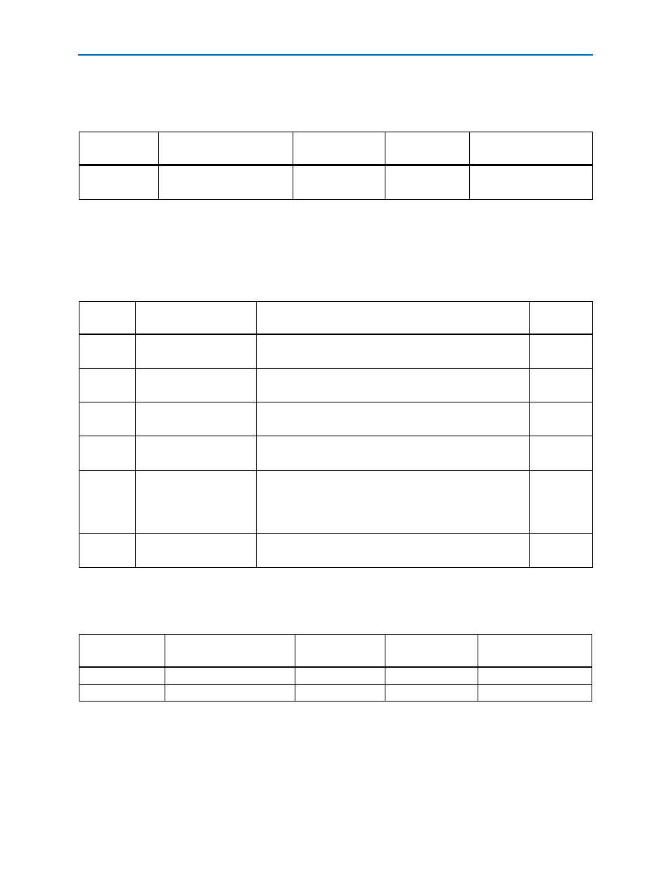
Table 2–15. Clock Enable DIP Switch Component Reference and Manufacturing Information
Board
Reference
Description
Manufacturer
Manufacturer
Part Number
Manufacturer Website
SW1
Four-Position slide DIP switch
C & K Components/
TTI Inc.
TDA04H0SB1
Table 2–16. JTAG Chain Jumper Controls
Board
Reference
Schematic Signal Name
Description
Default
J4
USB_DISABLEn
ON : Embedded USB-Blaster disable
OFF : Embedded USB-Blaster enable
OFF
J10
MAXII_JTAG_EN
ON : MAX II CPLD EPM2210 System Controller in-chain
OFF : Bypass MAX II CPLD EPM2210 System Controller
ON
J15
HSMA_JTAG_EN
ON : HSMA in-chain
OFF : Bypass HSMA
OFF
J5
HSMB_JTAG_EN
ON : HSMB in-chain
OFF : Bypass HSMB
OFF
J21
VCC_VCCL_SEL
ON (Pins 1 and 2) : VCC and VCCL = 0.9 V (if R126 is installed)
ON (Pins 2 and 3) : VCC and VCCL = 1.1 V (do not place the
shunt on these pins)
OFF : VCC and VCCL = 0.6 V (do not leave the shunt off)
ON (Pins 1
and 2)
J2
MSEL0
ON : Logic 0 is selected for MSEL
OFF : Logic 1 is selected for MSEL
ON
Table 2–17. JTAG Chain Jumper Component References and Manufacturing Information
Board Reference
Device Description
Manufacturer
Manufacturer
Part Number
Manufacturer Website
J2, J21
2×1 pin, 100 mil header
Samtec
TSW-103-08-G-S
J4, J5, J10, J15
2×1 pin, 2 mm header
Samtec
TMM-102-01-S-S