Flash, Flash –55 – Altera Stratix IV E FPGA Development Board User Manual
Page 63
Chapter 2: Board Components
2–55
Memory
May 2011
Altera Corporation
Stratix IV E FPGA Development Board Reference Manual
lists the SSRAM component reference and manufacturing information.
Flash
The flash interface consists of a single Numonyx StrataFlash embedded memory
device, providing 64-MB memory interface with a 16-bit data bus. This device is part
of the shared FSM bus which connects to the flash memory, SSRAM, and MAX II
CPLD EPM2210 System Controller.
The parameter blocks of this device are located at the bottom of the address space. The
parameter blocks are 32 K and main blocks are 128 K.
This 16-bit data memory interface can sustain burst read operations at up to 52 MHz
for a throughput of 832 Mbps. The write performance is 125 µs for a single word and
440 µs for a 32-word buffer. The erase time is 400 ms for a 32 K parameter block and
1200 ms for a 128 K main block.
U3.C11
Data bus parity lane 1
SSRAM_DQP1
2.5-V
—
—
U3.C1
Data bus parity lane 2
SSRAM_DQP2
—
—
U3.N1
Data bus parity lane 3
SSRAM_DQP3
—
—
U3.B7
Global write enable
SSRAM_GWn
—
U10.E11
U3.R1
Mode
SSRAM_MODE
—
U10.D11
U3.B8
Output enable
SSRAM_OEn
A22
—
U3.H11
Sleep
SSRAM_ZZ
—
U10.A13
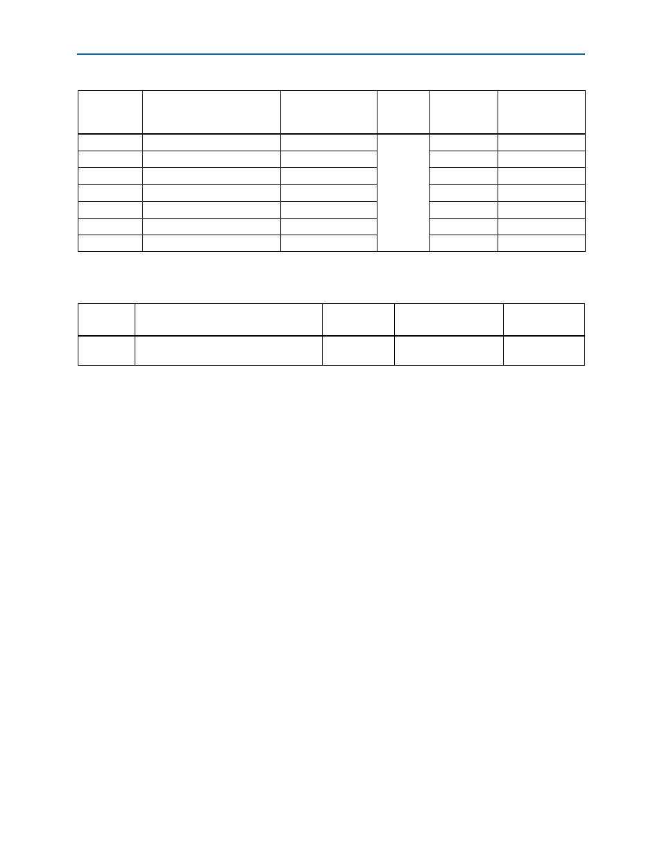
Table 2–49. SSRAM Pin Assignments, Schematic Signal Names, and Functions (Part 3 of 3)
Board
Reference
Description
Schematic Signal
Name
I/O
Standard
Stratix IV E
Device
Pin Number
Other Connections
Table 2–50. SSRAM Component Reference and Manufacturing Information
Board
Reference
Description
Manufacturer
Manufacturing
Part Number
Manufacturer
Website
U3
250 MHz standard synchronous pipelined
SCD static RAM, 512K × 36, BGA-165
ISSI Inc.
IS61VPS51236A-250B3