Altera Stratix IV E FPGA Development Board User Manual
Page 37
Chapter 2: Board Components
2–29
General User Input/Output
May 2011
Altera Corporation
Stratix IV E FPGA Development Board Reference Manual
shows the character LCD pin definitions, and is an excerpt from the Lumex
data sheet.
f
For more information such as timing, character maps, interface guidelines, and other
related documentation, visi
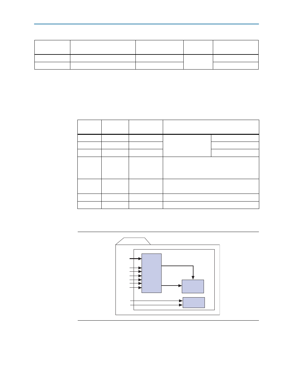
shows the functional block diagram of the Lumex LCD display.
1
The particular model used does not have a backlight.
J23.13
LCD data bus
LCD_DATA6
2.5-V
AE15
J23.14
LCD data bus
LCD_DATA7
AF15
Table 2–32. Character LCD Header Pin Assignments, Schematic Signal Names, and Functions
Board Reference
Description
Schematic Signal Name
I/O Standard
Stratix IV E Device
Pin Number
Table 2–33. Character LCD Pin Definitions and Functions
Pin
Number
Symbol
Level
Function
1
V
DD
—
Power supply
5 V
2
V
SS
—
GND (0 V)
3
V
0
—
For LCD drive
4
RS
H/L
Register select signal
H: Data input
L: Instruction input
5
R/W
H/L
H: Data read (module to MPU)
L: Data write (MPU to module)
6
E
H, H to L
Enable
7–14
DB0–DB7
H/L
Data bus, software selectable 4-bit or 8-bit mode
Figure 2–7. Character LCD Display Block Diagram
Block Diagram
16 X 2, 1/16 Duty, 1/5 Bias
E
SEC 80
COM 16
R/W
RS
DB[7:0]
LCD
Panel
LCD
Controller
LSI
and
Driver
LED Backlight
A
K
V
DD
V
SS
V
O