Altera PHYLite User Manual
Page 35
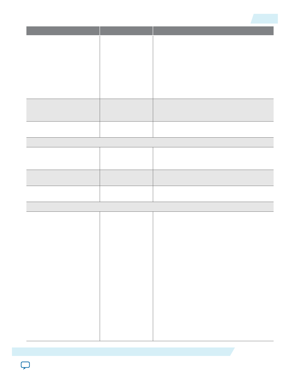
GUI Name
Values
Description
Read latency
1 to 63 external
interface clock cycles
Expected read latency of the external device in
memory clock cycles. The value is set to 4 by
default.
For example, a design with an external clock
frequency of 533 MHz in half-rate has a valid read
latency range of 5 to 63 external interface clock
cycles.
Refer to
.
Swap capture strobe polarity
—
Internally swap the negative and positive capture
strobe input pins. This feature is only available for
complementary strobe configurations.
Capture strobe phase shift
0,45,90,135, 180
Phase shift of input strobe relative to input data.
The value is set to 90° by default.
Group
0 to 3 (maximum
value is dependent on
the rate)
Additional delay added to the output data in
memory clock cycles.
Use output strobe
—
Use an output strobe. This option is enabled by
default.
Output strobe phase
0,45,90,135,180
Phase shift of the output strobe relative to the
output data. The value is set to 90° by default.
Group
Single ended,
Differential,
Complementary
Select the type of strobe. A single ended strobe
uses one pin, which will reduce the maximum
possible number of data pins in the group to 47.
Differential/complementary strobe types use 2
pins, which will reduce the maximum possible
number of data pins in the group to 46.
The value is set to Single ended by default.
Note: The differential strobe configuration
uses a differential input buffer, which
produces a single clock for the capture
DDIO and read FIFO. The complemen‐
tary strobe configuration uses two
single-ended input buffers and clocks
the data into the capture DDIO and
read FIFO using both clocks (as
required by protocols such as QDRII).
The output path functionality is the
same.
ug_altera_phylite
2015.01.16
Parameter Settings
35
Altera PHYLite for Parallel Interfaces IP Core User Guide
Altera Corporation