Timing components, Timing constraints and files – Altera PHYLite User Manual
Page 17
Timing Components
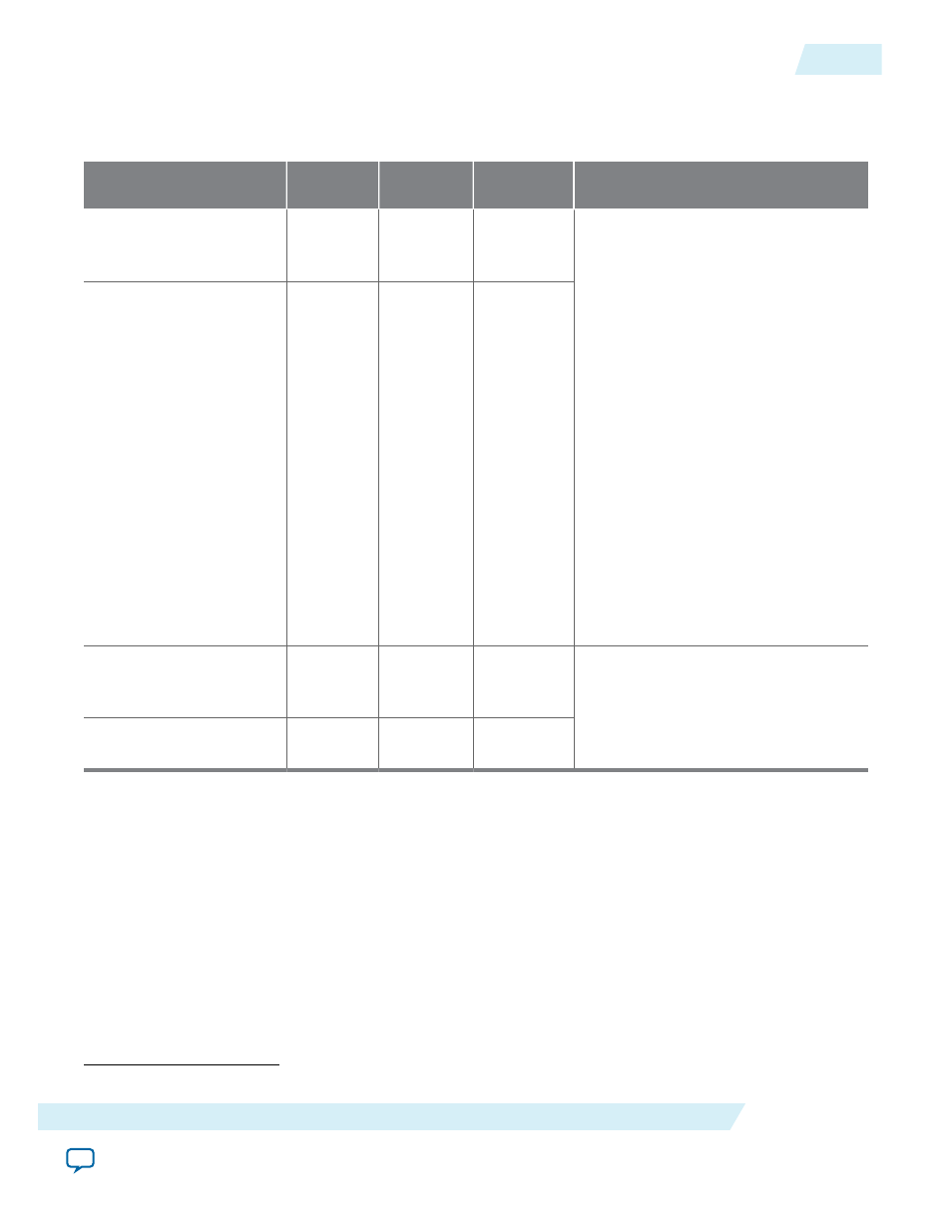
Table 9: Timing Components
Circuit Category
Timing
Paths
Source
Destination
Description
Source Synchronous
and optionally
calibrated
(2)
Read Path
Memory
Device
DQ Capture
Register
Source synchronous timing paths—
paths where clock and data signals are
passed from the transmitting devices
to the receiving devices.
Optionally calibrated paths—paths
with delay elements that are
dynamically reconfigurable to achieve
timing closure, especially at higher
frequency, and to maximize the
timing margins. You can calibrate
these paths by implementing an
algorithm and turning on the
optional dynamic reconfiguration
feature. An example of the calibrated
path is the FPGA to memory device
write path, in which you can
dynamically reconfigure the delay
elements to, for instance, compensate
the skew due to process voltage
temperature variation.
Source Synchronous
and optionally
calibrated
(2)
Write Path FPGA DQ/
DQS
Memory
Device
Internal FPGA
Core to
PHYLite
Path
Core
Registers
Write FIFO
The internal FPGA paths are paths in
the FPGA fabric. The TimeQuest
timing analyzer reports the
corresponding timing margins.
Internal FPGA
PHYLite to
Core
Read FIFO
Core
Registers
Timing Constraints and Files
To enable you to successfully timing constrain the Altera PHYLite for Parallel Interfaces IP core, the IP
core generates a set of timing files. You can locate these timing files in the
•
•
•
(2)
Can be optionally calibrated by using dynamic reconfiguration.
ug_altera_phylite
2015.01.16
Timing Components
17
Altera PHYLite for Parallel Interfaces IP Core User Guide
Altera Corporation