Altera PHYLite User Manual
Page 23
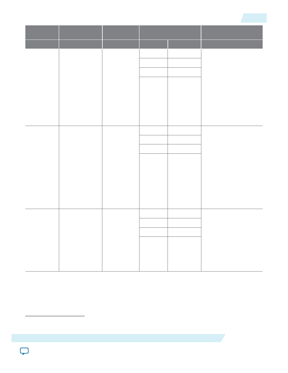
Feature
Avalon Address R/
W
Address CSR R
Control
Value
Field
Range
Strobe
PVT
compensat
ed input
delay
(3)
{id[3:0],
3'h2,lane_
addr[7:0],
4'hC,lgc_
sel[1:0],
3'h6,4'h0}
• lgc_sel[1:0] =
• 2'b01 for a
• 2'b10 for b
(4)
Not supported
Delay Value
9..0
Minimum Setting: 0
Maximum Setting: 1023
VCO clock periods
Incremental Delay: 1/
256th VCO clock period
Reserved
11..10
Enable
12
Reserved
31..13
Strobe
enable
phase
(3)
{id[3:0],
3'h2,lane_
addr[7:0],
4'hC,lgc_
sel[1:0],
3'h7,4'h0}
•
lgc_sel[1:0]
is:
• 2'b01 for a
• 2'b10 for b
(4)
•
{id[3:0],
3'h1,lane_
addr[7:0],
4'hC,
9'h194}
•
{id[3:0],
3'h1,lane_
addr[7:0],
4'hC,
9'h198}
Phase Value
12..0
Minimum Setting: Refer
Maximum Setting: Refer
Incremental Delay: 1/
128th VCO clock period
Reserved
14..13
Enable
15
Reserved
31..16
Strobe
enable
delay
(3)
{id[3:0],
3'h2,lane_
addr[7:0],4'hC,
9'h008}
{id[3:0],
3'h1,lane_
addr[7:0],
4'hC,9'h1A8}
Delay Value
5..0
Minimum Setting: 0
external clock cycles
Maximum Setting: 63
external memory clock
cycles
Incremental Delay: 1
external memory clock
cycle
Reserved
14..6
Enable
15
Reserved
31..16
(3)
Modifying these values must be done on all lanes in a group.
(4)
Strobe logic b is only used by the negative pin of complementary strobes.
ug_altera_phylite
2015.01.16
Addressing
23
Altera PHYLite for Parallel Interfaces IP Core User Guide
Altera Corporation