Input path data alignment – Altera PHYLite User Manual
Page 10
Operation
4
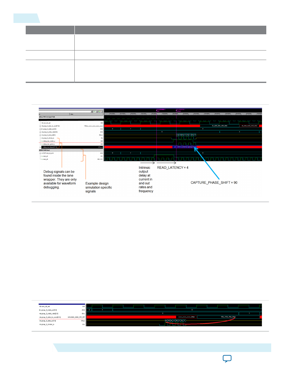
The strobe is optionally delayed to create a phase offset between the strobe and the
input data (for example, 90° phase shift for DDR center-alignment)
5
The data is clocked into the DDIO and read FIFO by the strobe
6
The VFIFO asserts the read enable on the read FIFO and the
rdata_valid
signal to
the core simultaneously. This outputs the captured data and the associated valid signal
to the core.
Figure 10: Input Path Waveform
This figure shows a waveform diagram of the input path.
Related Information
on page 40
For more information about input path signals
Input Path Data Alignment
The bus ordering of
data_to_core
,
rdata_en
, and
rdata_valid
is identical to the ordering of the output
path. That is, the LSBs of the bus hold the first time slice of data received.
The
rdata_valid
delay is always set by the IP core to match the
rdata_en
alignment. For example,
quarter-rate delays are multiples of four external memory clock cycles (one quarter rate clock cycle).
Unaligned reads will result in unaligned
rdata_valid
and
data_to_core
with
data
and
valid
signals
packed to the LSBs.
Figure 11: Example Input (Quarter Rate DDR) - Aligned
10
Input Path Data Alignment
ug_altera_phylite
2015.01.16
Altera Corporation
Altera PHYLite for Parallel Interfaces IP Core User Guide