Clocks – Altera PHYLite User Manual
Page 3
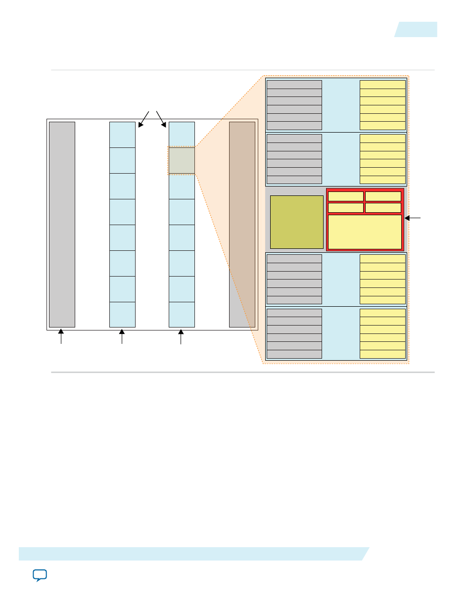
Figure 2: 48-I/O Banks in Arria 10 Devices
This figure shows a detailed view of the I/O bank in Arria 10 devices.
2L
2K
2J
2I
2H
2G
2F
2A
3H
3G
3F
3E
3D
3C
3B
3A
Transc
eiv
er B
lock
Transc
eiv
er B
lock
HSSI
Column
I/O
Column
Tile
Control
I/O
Column
Individual
I/O Banks
LVDS I/O Buffer Pair
LVDS I/O Buffer Pair
LVDS I/O Buffer Pair
LVDS I/O Buffer Pair
LVDS I/O Buffer Pair
LVDS I/O Buffer Pair
SERDES & DPA
SERDES & DPA
SERDES & DPA
SERDES & DPA
SERDES & DPA
SERDES & DPA
I/O Lane
LVDS I/O Buffer Pair
LVDS I/O Buffer Pair
LVDS I/O Buffer Pair
LVDS I/O Buffer Pair
LVDS I/O Buffer Pair
LVDS I/O Buffer Pair
SERDES & DPA
SERDES & DPA
SERDES & DPA
SERDES & DPA
SERDES & DPA
SERDES & DPA
I/O Lane
I/O Center
I/O PLL
Hard Memory Controller
and
PHY Sequencer
I/O DLL
I/O CLK
OCT
VR
LVDS I/O Buffer Pair
LVDS I/O Buffer Pair
LVDS I/O Buffer Pair
LVDS I/O Buffer Pair
LVDS I/O Buffer Pair
LVDS I/O Buffer Pair
SERDES & DPA
SERDES & DPA
SERDES & DPA
SERDES & DPA
SERDES & DPA
SERDES & DPA
I/O Lane
LVDS I/O Buffer Pair
LVDS I/O Buffer Pair
LVDS I/O Buffer Pair
LVDS I/O Buffer Pair
LVDS I/O Buffer Pair
LVDS I/O Buffer Pair
SERDES & DPA
SERDES & DPA
SERDES & DPA
SERDES & DPA
SERDES & DPA
SERDES & DPA
I/O Lane
Each I/O lane contains the DDR-PHY input and output path logic for 12 I/Os as well as a DQS logic
block. All four lanes in a bank can be combined to form a single data/strobe group or up to four groups in
the same interface. Under certain conditions, two groups from different interfaces can also be supported
in the same bank.
Related Information
•
For more information about placement restrictions
•
For more information about the architecture
Clocks
The Altera PHYLite for Parallel Interfaces IP core uses four clock domains for the output and input paths.
Refer to
for the clock domain boundaries.
ug_altera_phylite
2015.01.16
Clocks
3
Altera PHYLite for Parallel Interfaces IP Core User Guide
Altera Corporation