Table 12 – Altera PHYLite User Manual
Page 24
Feature
Avalon Address R/
W
Address CSR R
Control
Value
Field
Range
Read valid
delay
(3)
{id[3:0],
3'h2,lane_
addr[7:0],4'hC,
9'h00C}
{id[3:0],
3'h1,lane_
addr[7:0],
4'hC,9'h1A4}
Delay Value
6..0
Minimum Setting: 0
external clock cycles
Maximum Setting: 127
external memory clock
cycles
Incremental Delay: 1
external memory clock
cycle
Reserved
14..7
Enable
15
Reserved
31..16
Internal
VREF
Code
{id[3:0],
3'h2,lane_
addr[7:0],4'hC,
9'h014}
Not supported
VREF Code
5..0
Refer to
Reserved
(5)
31..6
(5)
Where:
•
id[3:0]
refers to the Interface ID parameter
•
lane_addr[7:0]
refers to the address of a given lane in an interface. This is set by the Fitter and can be
queried in the parameter table as described in the
•
pin[4:0]
refers to the physical location of the pin in a lane. A pin location is either determined by the
Fitter or through a .qsf assignment and can be queried in the parameter table as described in the
Note: For more information about calculating various clocking and delay calculations, depending on the
interface frequency and rate, refer to
.
Output and Strobe Enable Minimum and Maximum Phase Settings
When dynamically reconfiguring the interpolator phase settings, the values must be kept within the
ranges below to ensure proper operation of the circuitry.
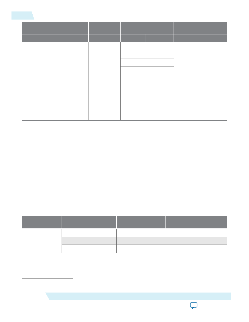
Table 12: Output and Strobe Enable Minimum and Maximum Phase Settings
VCO Multiplication
Factor
Core Rate
Minimum Interpolator
Phase
Maximum Interpolator Phase
1
Full
0x100
0xA80
Half
0x280
0xBC0
Quarter
0x180
0xA00
(5)
Reserved bit ranges must be zero
24
Output and Strobe Enable Minimum and Maximum Phase Settings
ug_altera_phylite
2015.01.16
Altera Corporation
Altera PHYLite for Parallel Interfaces IP Core User Guide