Setup with usb-to-serial adapter, Demonstration meter, 1 setup with usb-to-serial adapter – Maxim Integrated 71M6533-DB User Manual
Page 9

71M6533-
DB Demo Board User’s Manual
Page: 9 of 75
`
REV 3
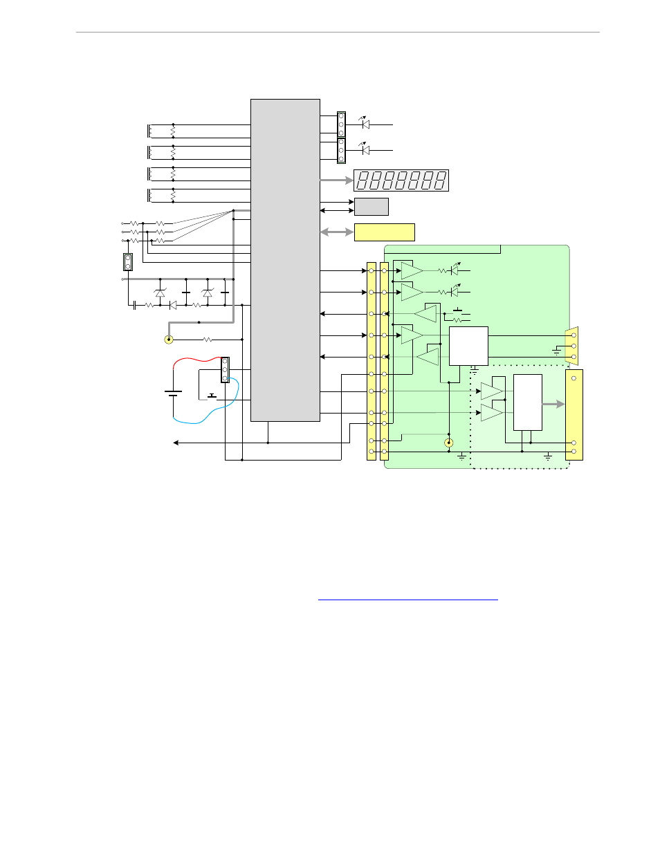
Figure 1-1: Block Diagram for the 71M6533-DB Demo Board with Debug Board
1.7.1 SETUP WITH USB-TO-SERIAL ADAPTER
The USB-to-Serial Adapter shipped with Demo Kits starting in June 2011 provides a connection to the Demo
Board via USB. The USB-to-Serial Adapter is plugged into connector J2 of the DB6533 as shown in Figure 1-2.
The PC should be running HyperTerminal or a similar serial interface program. A suitable driver, e.g. the FTDI
CDM Driver Package, must be installed on the PC to enable the USB port to be mapped as a virtual COM port.
The driver can be found on the FTDI web site
The USB-to-Serial Adapter is self-powered via the USB port on the PC.
DEMONSTRATION METER
IA
IB
IC
VC
VB
NEUTRAL
IAP
I B P
I C P
V3P3A
VC
VB
VA
3.3v
VA
GND
V3P3
GND
5V DC
EEPROM
ICE Connector
DIO56
DIO57
DIO58
TX
RX
DB9
to PC
COM Port
J5
68 Pin Connector
to NI PCI-6534
DIO Board
6533
Single Chip
Meter
TMUXOUT
CKTEST
3.3V LCD
DIO4
DIO5
I D P
INEUTRAL
External Current
Transformers
IAN
I B N
I C N
V3P3SYS
Wh
VARh
DIO6/WPULSE
DIO7/RPULSE
PULSE OUTPUTS
DIO9/YPULSE
DIO8/XPULSE
V3P3SYS
V3P3D
VBAT
PB
battery
(optional)
JP8
PB
On-board
components
powered by
V3P3D
OPTO
OPTO
OPTO
OPTO
OPTO
5V DC
V5_DBG
GND_DBG
V5_DBG
V5_DBG
RS-232
INTERFACE
GND_DBG
V5_DBG
OPTO
OPTO
FPGA
04/25/2008
V5_NI
CE HEARTBEAT (1Hz)
MPU HEARTBEAT (5Hz)
DEBUG BOARD (OPTIONAL)
RTM INTERFACE
JP21
J2
N/C
N/C
4
15, 16
13, 14
6
6
8
12
10
3
1
2
5, 7,
9, 11
GND
V3P3SYS
JP1
I D N
