Hardware description, Table 3-1: 71m6533-db demo board description, 3hardware description – Maxim Integrated 71M6533-DB User Manual
Page 55
71M6533-
DB Demo Board User’s Manual
Page: 55 of 75
`
REV 3
3
HARDWARE DESCRIPTION
3.1 71M6533-DB DEMO BOARD DESCRIPTION: JUMPERS, SWITCHES
AND TEST POINTS
The items described in the following tables refer to the flags in Figure 3-1.
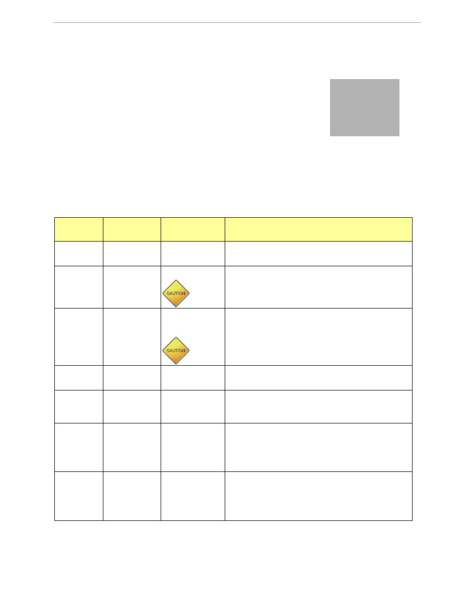
Item #
Reference
Designator
Name
Use
1, 2, 6
TP2, TP4, TP6
VA, VB, VC
Two-pin header test points. One pin is the VA, VB, or VC
line voltage input to the IC and the other end is V3P3.
4
JP1
PS_SEL[0]
A jumper is placed across JP1 to activate the internal
power supply. JP1 is on the bottom of the board.
Caution: High Voltage! Do not touch!
3, 8, 11
J4, J6, J8
VA_IN, VB_IN,
VC_IN
VA_IN, VB_IN, and VC_IN are the line voltage inputs to the
board. Each input has a resistor divider that leads to the
pin on the IC associated with the voltage input to the ADC.
These inputs are spade terminals mounted on the bottom
of the board.
Caution: High Voltage! Do not touch these pins!
5
J9
NEUTRAL
The NEUTRAL voltage input connected to V3P3. This input
is a spade terminal mounted on the bottom of the board.
7
SW2
RESET
Chip reset switch: When the switch is pressed, the RESET
pin of the IC is pulled high which resets the IC into a known
state.
9
JP8
VBAT, GND
Three-pin header that allows selection of power to the
VBAT pin. When the jumper is placed between pins 1 and
2 (default setting of demo board) VBAT is tied to the IC
supply. An external battery can be connected between
terminals 2 and 3.
10
SW3
PB
Pushbutton connected to the PB pin on the IC. This push-
button can be used in conjunction with the Demo Code to
wake the IC from sleep mode or LCD mode to brown-out
mode. In mission mode, the pushbutton serves to cycle the
LCD display.
Table 3-1: 71M6533-DB Demo Board Description
3