Maxim Integrated 71M6533-DB User Manual
Page 72
71M6533-
DB Demo Board User’s Manual
Page: 72 of 75
REV 3
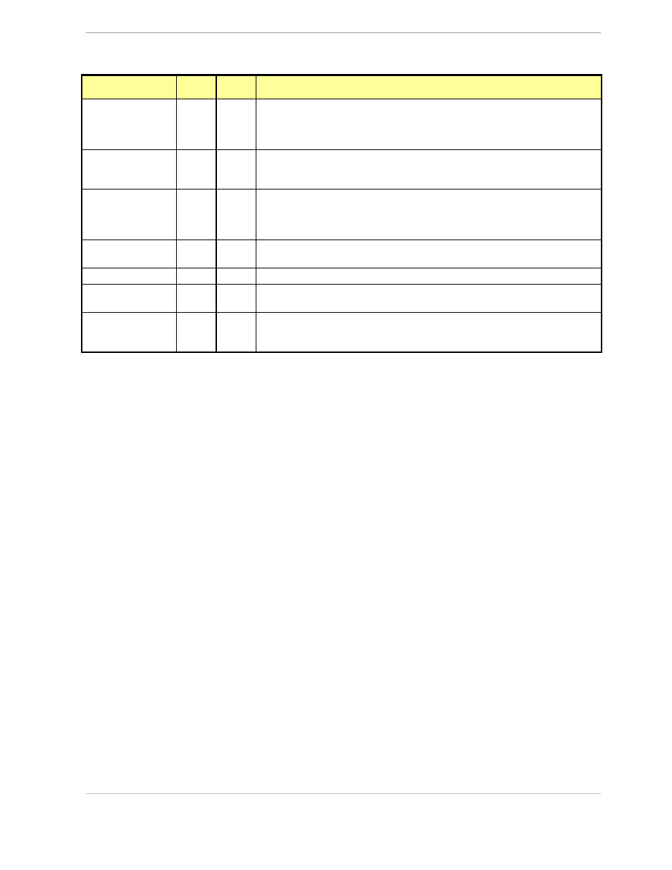
Name
Type
Pin #
Description
OPT_RX/DIO1
I/O
91
Multi-use pin, configurable as either Optical Receive Input or general DIO.
When configured as OPT_RX, this pin is a regular UART RX pin. If this pin
is unused it must be configured as an output or tied to V3P3D or
GNDD.
OPT_TX/DIO2
I/O
3
Multi-use pin, configurable as either Optical LED Transmit Output. When
configured as OPT_TX, this pin is capable of directly driving an LED for
transmitting data in an IR serial interface.
RESET
I
74
Chip reset: This input pin is used to reset the chip into a known state. For
normal operation, this pin is pulled low. To reset the chip, this pin should be
pulled high. This pin has an internal 30μA (nominal) current source pull-
down. No external reset circuitry is necessary.
RX
I
71
UART input. If this pin is unused it must be configured as an output or
tied to V3P3D or GNDD.
TX
O
5
UART output.
TEST
I
94
Enables Production Test. This pin must be grounded in normal
operation.
PB
I
97
Push button input. Should be at GND when not active. A rising edge sets
the IE_PB flag. It also causes the part to wake up if it is in SLEEP or LCD
mode. PB does not have an internal pull-up or pull-down resistor.
Table 4-4: 71M6533/71M6533H Pin Description Table 3/3
Pin types: P = Power, O = Output, I = Input, I/O = Input/Output