71m6533 pin-out information – Maxim Integrated 71M6533-DB User Manual
Page 70
71M6533-
DB Demo Board User’s Manual
Page: 70 of 75
REV 3
4.4 71M6533 PIN-OUT INFORMATION
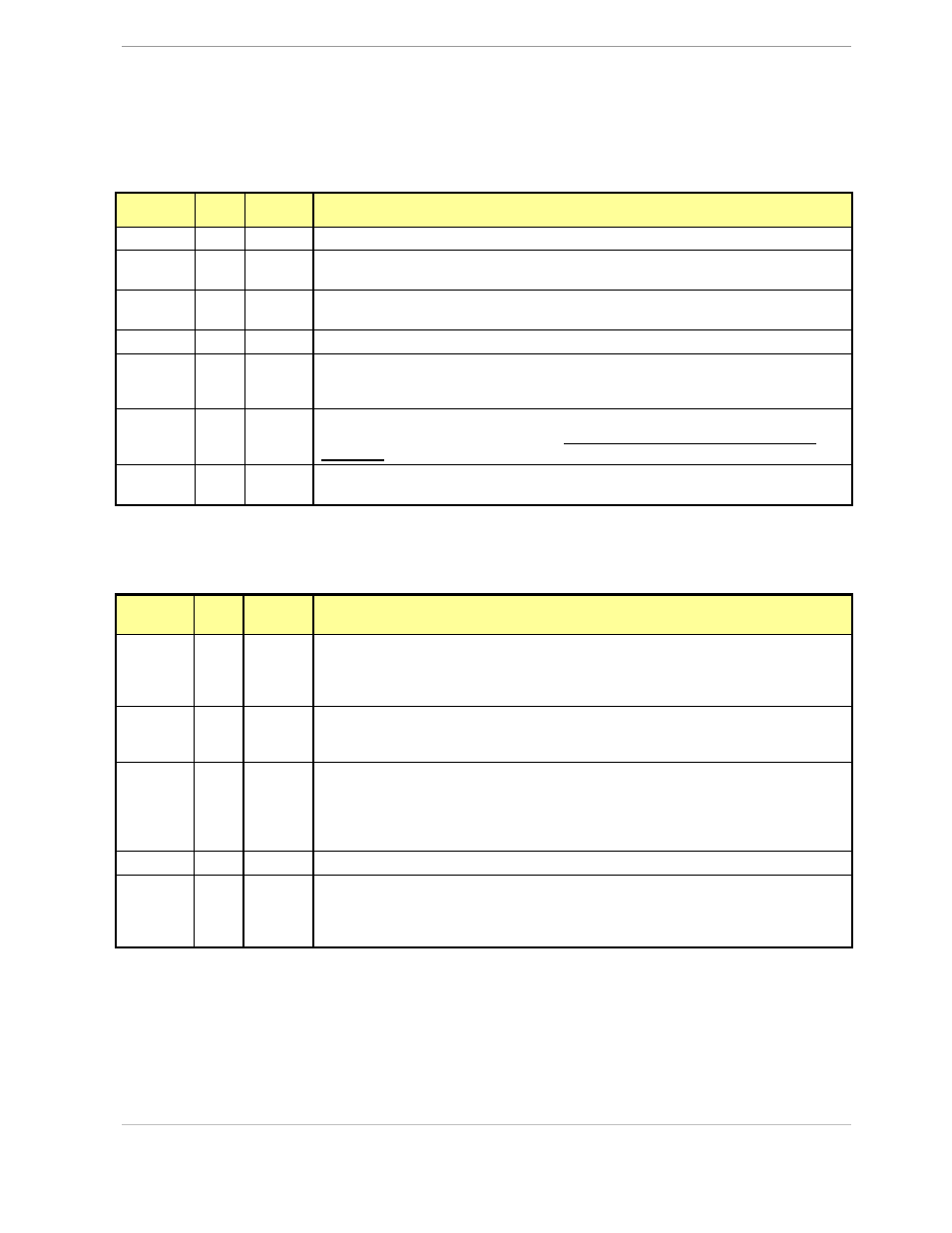
Power/Ground/NC Pins:
Name
Type Pin #
Description
GNDA
P
76
Analog ground: This pin should be connected directly to the ground plane.
GNDD
P
1, 39,
75, 92
Digital ground: This pin should be connected directly to the ground plane.
V3P3A
P
77
Analog power supply: A 3.3V power supply should be connected to this pin. V3P3A
must be the same voltage as V3P3SYS.
V3P3SYS
P
9
System 3.3V supply. This pin should be connected to a 3.3V power supply.
V3P3D
P
7
Auxiliary voltage output of the chip, controlled by the internal 3.3V selection switch.
In mission mode, this pin is internally connected to V3P3SYS. In BROWNOUT
mode, it is internally connected to VBAT. This pin is floating in LCD and sleep mode.
VBAT
P
72
Battery backup power and oscillator supply. A battery or super-capacitor is to be
connected between VBAT and GNDD. If no battery is used, connect VBAT to
V3P3SYS.
V2P5
O
73
Output of the internal 2.5V regulator. A 0.1µF capacitor to GNDA should be
connected to this pin.
Table 4-2: 71M6533/71M6533H Pin Description Table 1/3
Analog Pins:
Name
Typ
e
Pin #
Description
IAP/IAN,
IBP/IBN,
ICP/ICN,
IDP/IDN
I
88,87,
86,85,
84,83,
82,81
Differential Line Current Sense Inputs: These pins are voltage inputs to the internal
A/D converter. Typically, they are connected to the outputs of current sensors.
Unused pins must be tied to V3P3A. IDP/IDN are additional Line Current Sense
Input pins.
VA,
VB,
VC
I
80,
79,
78
Line Voltage Sense Inputs: These pins are voltage inputs to the internal A/D
converter. Typically, they are connected to the outputs of resistor dividers. Unused
pins must be tied to V3P3A.
V1
I
90
Comparator Input: This pin is a voltage input to the internal comparator. The voltage
applied to the pin is compared to an internal BIAS voltage (1.6V). If the input voltage
is above the reference, the comparator output will be high (1). If the comparator
output is low, a voltage fault will occur. A series 5k
resistor should be connected
from V1 to the resistor divider.
VREF
O
89
Voltage Reference for the ADC. This pin should be left unconnected (floating).
XIN
XOUT
I
93,
95
Crystal Inputs: A 32kHz crystal should be connected across these pins. Typically, a
33pF capacitor is also connected from XIN to GNDA and a 15pF capacitor is
connected from XOUT to GNDA. It is important to minimize the capacitance bet-
ween these pins. See the crystal manufacturer datasheet for details.
Table 4-3: 71M6533/71M6533H Pin Description Table 2/3